SLT Enables Test Content to Shift Right to Optimize Test Efficiency and Part Quality
By Dave Armstrong and Davette Berry, Directors of Business Development, and Craig Snyder, Business Development Manager
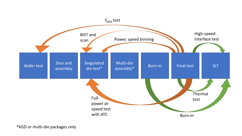
Increasing device complexity and the continuing drive for higher levels of quality are fostering a reconsideration of test strategies. To be effective, test engineers must choose how to optimally deploy test content, from wafer probing to system-level test (SLT). A March 2019 TestConX presentation1 outlines how test content is typically allocated—for example, final test performs structural and functional tests, parametric measurements, and performance binning; burn-in screens for early-life failures; and SLT looks for mission-mode failures resulting from hardware and software interactions. For cost balancing, though, it might be preferable to transfer a test step that has traditionally been performed at final package test, for example, upstream toward wafer test or downstream to SLT. At Advantest, we call the upstream transfer “shift left” and the downstream transfer “shift right” (Figure 1).

Figure 1. The test flow from wafer probing to SLT offers opportunities to shift test content right or left to optimize test efficiency and part quality.
Shift left overview
A January-February article2 in Chip Scale Review describes the shift left process, which is particularly applicable to the integration of heterogeneous known-good die (KGD). For KGD test, it is advantageous to shift test content left from final test toward wafer test or to a singulated-die test stage, where you can perform full-power active-thermal-control (ATC) testing at speed. For KGD, a shift left strategy of more testing sooner reduces the number of good die scrapped because of one bad part in a multi-die assembly, ultimately leading to lower costs and more profit.
SLT overview
Alternatively, other applications can benefit from a shift right strategy, in which some test steps are transferred from final test and burn-in toward SLT, especially as SLT becomes more pervasive in manufacturing test.
SLT mimics in a manufacturing test environment the real-world operating conditions of the device under test, as described in a September 2020 GO SEMI & BEYOND article. In SLT, the device under test interacts with its mission-mode software and communicates with peripheral devices including power-management ICs (PMICs), DRAMs, and high-speed interfaces including USB or PCIe gen 4. Originally focused primarily on the memory and storage market during early silicon bring-up, SLT has expanded to include test of high-end processors and systems on chips (SoCs) used in computing, mobile, and automotive markets as well.
In addition to expanding to more markets, SLT is increasingly being applied to 100% of manufactured parts—not just samples. 100% SLT opens the door for a shift right of many test functions from final test to an enhanced SLT stage. This shift may also result in a lower overall cost of test.
High-speed interface test
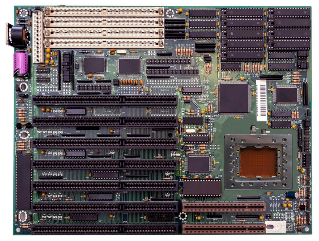
One opportunity for the shift right of test content from final test to enhanced SLT involves connectivity and the test of high-speed I/O, but high-speed I/O tests bring about key challenges. In mission mode, a device will likely be soldered to a printed-circuit board close to its peripheral circuitry or inserted into an OEM socket on a computer motherboard. Neither is possible in the manufacturing test environment of SLT.
In SLT, connectivity and signal degradation problems—not defective devices—cause significant first-pass yield problems, seriously compromising throughput due to retest.
What’s needed is a high-performance, high-durability test socket for use in SLT that provides an optimized, tuned interconnect between the chip under test and its peripheral circuitry. To that end, Advantest in January 2020 acquired Essai, a supplier of semiconductor final-test and SLT test sockets (Figure 2) and thermal-control units. Essai possesses the expertise to design and manufacture the sockets with ever smaller pitches and ever higher electrical and thermal performance to address the final-test and SLT needs for successive generations of chips. These sockets permit at-speed test of high-speed interfaces at SLT, thereby enabling full-speed system level testing.

Figure 2. A test socket suitable for SLT provides mechanical durability while supporting an optimized signal path from the device under test to its peripheral components.
In addition, the socketed SLT motherboard enables a more native environment configuration for the device under test and better represents real-world conditions than does a typical ATE final test insertion, where propagation delays related to the path from device through the socket and load board and finally to the instrument must be taken into account.
Thermal test
Almost all of Advantest’s SLT customers are testing device behaviors at different temperatures at some point in the test flow, and most, if not all, of these tests can be shifted right to the SLT environment.
An example in the automotive industry is the cold-boot requirement to ensure that vehicle electronics will boot up on an Alaskan winter morning.
SLT can exercise a device at high temperatures, too. Many devices have temperature sensors, which may trigger a processor at a certain temperature to communicate with a PMIC to initiate a low-power operating mode until the temperature returns to normal.
Testing across temperature ranges presents its own challenges. For example, when you subject the device to different temperatures you are also subjecting the interconnect to different temperatures, leading to potential failures due to expansion and contraction. One solution is to get the device to temperature while leaving the rest of the SLT environment at as neutral a temperature as possible. Further, with heterogeneous integration, a substrate which may be as large as 100 mm on a side may accommodate multiple die, each with its own thermal response and challenge. Such a package might require topside contact by a thermal interposer that maintains temperature setpoints within different zones, all within that same package.
Burn-in
Finally, burn-in is a common test insertion for both automotive and high-performance compute devices. SLT test times extend from less than a minute to tens of minutes, and burn-in times extend from tens of minutes to hours. Given that the burn-in and SLT test insertions require some common thermal stress infrastructure, Advantest can enable the automation of combining SLT and burn-in in a common test cell. With some customers exploring high-speed I/O test during burn-in, burn-in can offer another opportunity to shift test content right.
Conclusion
Ultimately, in addition to its role mimicking the device under test’s mission mode, SLT is an opportunity to shift test content right. What it is not is an opportunity to completely replace other test steps. There will always be a need for final test, covering at a minimum short/open test to find assembly defects and performing multi-die communications checks and/or parametric measurements. On the other hand, the SLT test often includes creative interconnect solutions to high-speed memory, which require a test environment that would be impossible on an ATE system.
Committing to SLT for 100% of devices is a big step for companies to take, but once they do so they find that they can simplify final test by reducing test redundancy while continuing to ensure, and potentially enhance, the level of quality. Advantest serves the entire semiconductor manufacturing test space, from wafer probe to SLT. Advantest engineers stand ready to work with customers to determine the optimum deployment of test resources for their specific applications.
References
- Berry, Davette, et al., “Holistic approach to test coverage across Final Test, Burn In, and System Level Test,” TestConX, Mesa, AZ, March 3-6, 2019.
https://www.testconx.org/premium/wp-content/uploads/2019/TestConX20193ap2_5612.pdf
- Armstrong, Dave, “Heterogeneous integration prompts test content to ‘shift left,’” Chip Scale Review, January-February 2021, p. 7.
https://chipscalereview.com/wp-content/uploads/2021/01/ChipScale_Jan-Feb_2021-digital.pdf - Pizza, Fabio, “System-Level Test Methodologies Take Center Stage,” GO SEMI & BEYOND, September 27, 2020.
https://www.gosemiandbeyond.com/system-level-test-methodologies-take-center-stage/


