Editor's note: This article is based on the poster "The Age of Singulated Die Test" presented at the Test Vision Symposium held in conjunction with SEMICON West, October 7-9, 2025, Phoenix, AZ.
By Brent Bullock, Advantest America
The accelerating rate at which the industry adopts new process nodes is posing critical test challenges. Shrinking geometries combined with increased design complexity with respect to metrics such as gates per square micrometer, plus higher operating frequencies, are leading to ever higher levels of power density. The resulting device thermal excursions are driving the need for singulated die test (SDT) with active thermal control (ATC), which combine to boost yields and ensure the quality of the chiplets and other die that make up multichip packages for high-performance computing (HPC) and artificial-intelligence (AI) server farms.
SDT detects defects that do not appear until after singulation, which are most often faults in chip-to-chip interconnects. SDT can also improve device handling efficiency, so it is applicable to multiple test scenarios, with test content varying accordingly:
- Die-probe insertion using Final-Test conditions
- Die matching and die-bank rescreening
- Complex chip-on-wafer/ known-good assembly testing
- Extended yield learning
- Silicon-photonics optical-engine testing
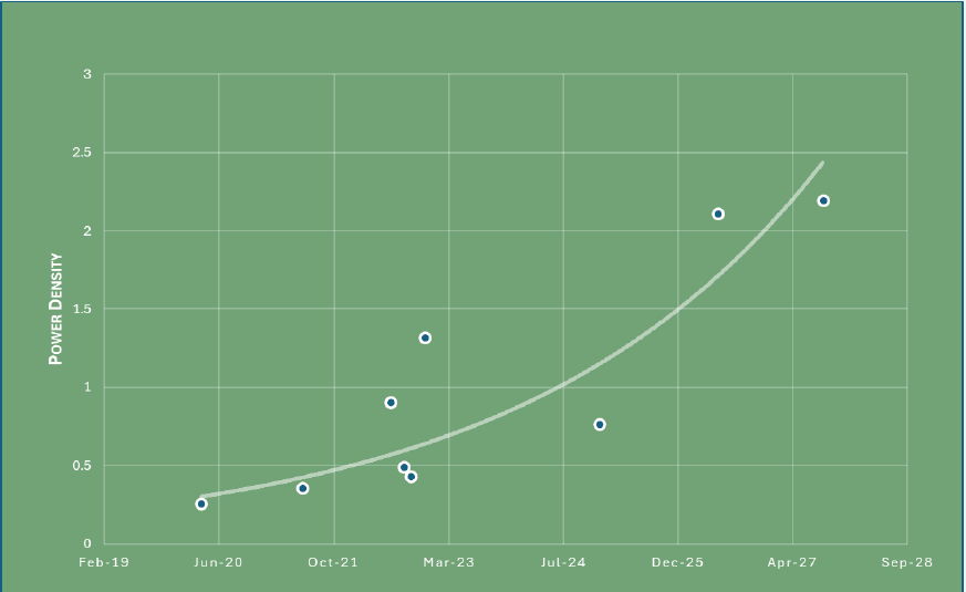
Power-density growth
Figure 1 shows an estimate of power density's dramatic growth in the HPC/AI era.
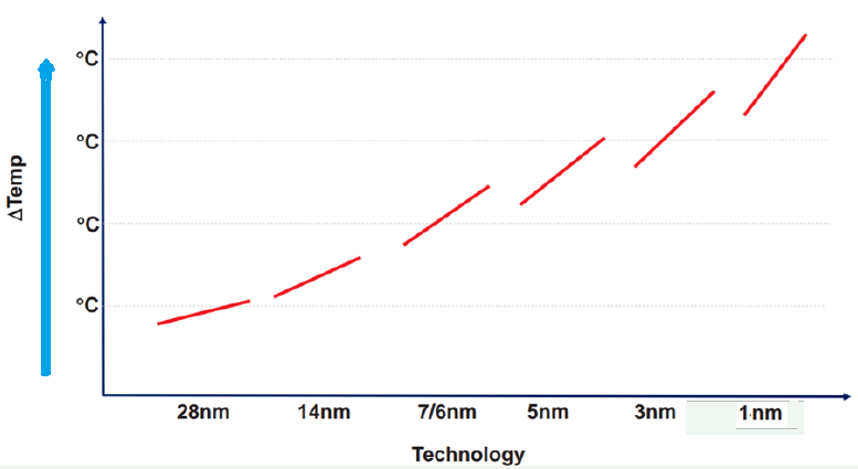
The high power density in turn produces large thermal gradients, with the low to max temperature changes increasing dramatically in both mission mode and test mode as process geometries shrink, as shown in Figure 2. These large temperature gradients lead to increased yield loss due to challenges in maintaining the set temperature.
Consequently, Advantest customers are taking steps to monitor and control the thermal gradients and respond to the temperature excursions from the wafer-sort level through final test.
However, the ability to control thermal behavior during various test insertions has been problematic, requiring close attention to the thermal interfaces and differing thermal masses. Thermal control at wafer sort traditionally has been very limited, because a single large chuck, historically with just a single sensor in the middle of it, provides temperature control. Subsequent chuck configurations included multiple sensors in multiple zones, approaches that did provide some relief and drove yield improvements. Package test also presents challenges, because the package itself, potentially with a lid, adds thermal mass. So many customers feel they need to move to more aggressive thermal-control solutions at die sort.
Die-probe insertion
Die-probe insertion offers one solution, with thermal control required for only a small piece of the wafer---the singulated die---allowing thermal interfacing directly without a lid, so the thermal mass is very low and the thermal characteristics very different. With the arrival of high-power-density devices, SDT, which has existed since about 2015 but has found limited adoption, is now gaining interest.
SDT allows customers to respond to temperature changes very quickly, and Advantest has been involved in studies in this area. In particular, customers have CoWoS and similar advanced package assemblies, and many defects in such structures do not appear until after the singulation process, which applies mechanical stress to each die. Furthermore, temperature stresses for singulated dies can be greater because each singulated chip cannot rely on the mass of the entire wafer, which provides mechanical strength and thermal dissipation. The combination of mechanical and thermal stresses increases the chances of faults at the die-to-die interconnects, whether in CoWoS assemblies or HBM stacks. The latter continues to present yield challenges as stack heights continue to grow.
There are several benefits to singulated die test. The main focus is on temperature response---the ability to regulate thermal excursions during a wafer-sort insertion by mimicking the final-test conditions. Some Advantest customers have a discrepancy between final-test temperature and wafer-sort temperature set points because the wafer-probe environment has been more challenging. The singulated die probe allows better control to mitigate the thermal excursions and probe burn risk that are more common with typical chuck-based probe insertions. With the rise of chiplet technology and stacked-die use, it is increasingly likely that good dies can be mixed with bad dies, resulting in good dies, substrates, and interposers being discarded.
SDT can also accelerate product release cycles, speeding time to market. With traditional wafer probing, a few bad dies can hold up a complete wafer as engineers study yield problems and determine how to fix them. With SDT, bad dies can be held back for study, but good dies can immediately proceed on to packaging and final test and on to customers.
Traditional wafer probing is also subject to probe-burn concerns that arise when touching down on multiple dies, especially in the early phases of a new design or process node. SDT can also avoid the silicon defectivity problems that compromise multi-site probe test efficiency by matching probably good die.
Die-level handler
Equipment that can address the challenges of singulated die test includes the Advantest HA1200 die-level handler, which, when equipped with an active thermal interface (ATI), can be used in conjunction with test systems such as the Advantest V93000 SoC tester. The combination can enable the test of high-end SoCs with excellent test coverage, helping to reduce yield loss at the final test of multi-die assembled products. Figure 3 shows the HA1200 (left) and a 100-W/cm2 quad-site active thermal interface for testing CPU chiplet dies. When used with the V93000, which sits on top of the HA1200's die alignment unit (right-side module below), the handler and thermal interface can obtain a thermal profile to enable comparison with the thermal profiles at wafer sort and at final test.
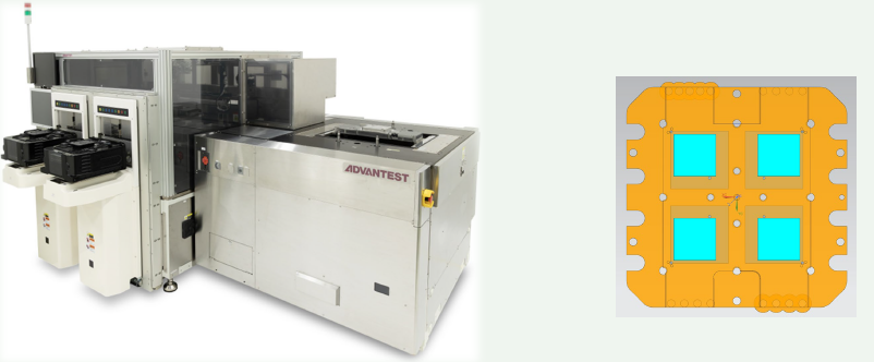
Figure 3. An Advantest study employed an HA1200 handler (left) and a 100-W/cm2 quad-site active thermal interface (right).
A specific study conducted by Advantest included an analog-to-digital converter attached to the probe load board to capture profiles of device current, voltage, and junction temperature; an HA1200 die-level handler configured with two generations of the company's ATI thermal solution; and a V93000 tester programmed to test a 6-nm CPU chiplet die.
The study involved manual execution of a single test-site V93000 test flow on a quad-site die-probe setup using a hot temperature setpoint, and it compared the temperature profiles of a hot-temperature wafer-sort insertion, a hot-temperature package-test insertion, and two hot-temperature SDT insertion. Figure 4 shows the peak temperature excursion and the time to guardband for the wafer-sort hot test, two test setups for the SDT hot test (Thermal setup #1 with the Gen 1 ATI solution and Thermal setup #2 with the Gen 2 version), and the final package test hot test.

Further work
Work remains to be done on effectively implementing SDT. For example, customers are very interested in applying SDT to achieve SoCoW-assembly quality improvements. Also of interest are new, larger Advantest thermal interfaces that can dissipate more heat. Work needs to be done evaluating these interfaces based on customer data, as power density increases with future process nodes. In addition, work is proceeding on multisite efficiency gains and quad-site thermal evaluation, as well as on studying post-singulation yield and defectivity.
Finally, customers are evaluating when and for what devices SDT is most effective. Most customers are expected to continue with the Wafer Sort 1 cold test, but they could consider replacing the Wafer Sort 2 chuck-based test with SDT, allowing closer tuning with final-test results. These customers must evaluate trade-offs between yield gains and disruption to their standard test processes and the capital investment involved. Considerations will include factors such as total test time and the average selling price of the device under test. For many customers producing singulated chip on wafer structures, SDT will very likely pay for itself.
Conclusion
Advantest's HA1200 handler equipped with ATC has demonstrated the ability to precisely regulate temperatures, allowing a singulated die test to simulate final-test conditions. An Advantest study has demonstrated that SDT is effective in controlling temperatures as process geometries shrink and power densities rise for HPC and AI devices with HBM stacks and CoWoS structures.
Acknowledgements
Advantest team members in Japan, Taiwan, Singapore, and the U.S.A. contributed to this work.