Pages Menu
Categories Menu

Posted in Top Stories

HSIO Loopback Turns Challenges into Opportunities for Test at 112 Gbps

By Dave Armstrong, Principal Test Strategist, Advantest, and Don Thompson, Senior Director of Engineering, R&D Altanova

For both PCIe and Ethernet (IEEE 802.3) signals are getting mighty small. With PCIe 5 reaching 32 Gbps (NRZ at 32 GBaud) and 802.3 reaching 112 Gbps (PAM4 at 56 GBaud), typical eye-mask limits are shrinking. Consequently, test requirements for high-speed I/O (HSIO) test are becoming daunting.

HSIO test involves measurement of Tx eye height and width, confirmation that a receiver can detect a low-level signal, and confirmation that continuous time linear equalization (CTLE) is effectively compensating for insertion loss. In addition, the test must verify bit error rate and confirm that a receiver can receive an off-frequency or out-of-phase signal. Yet another requirement is DC access for continuity and scan test.

Traditionally, HSIO loopback has been the preferred approach to HSIO test, with a simple wire or capacitor connecting a DUT’s Tx to Rx inputs. Loopback itself comes in various forms. The simplest form is internal loopback in which the device talks to itself and never exercises the transceiver circuitry; it can test internal logic only.

Another method is AC-coupled external loopback which does exercise the I/O circuitry, but like internal loopback, it does not perform Tx/Rx eye tests, and it does not test pre-emphasis and equalization. AC-coupled loopback is easy to lay out on a DUT board, but the signal level the Rx receives is too low loss / too hot, making the test too easy. Similarly, when connecting channel pairs for loopback tests, the Tx/Rx pairs share the same PLL/DLL, again making the test too easy. 

There are some workarounds that can be used on an AC-coupled external loopback. Long circuit-board trace lengths could help make AC-coupled test more realistic, while connecting the Tx of one signal pair bank to the Rx of another would mitigate the problems of a shared PLL/DLL. And the addition of bias tees loopback circuits would support DC and continuity (Figure 1).

Figure 1. AC-coupled external loopback test with bias tees for DC test.

However, these loopback tests do not provide sufficient visibility into the DUT that would aid in diagnosis, making them ineffective, particularly at speeds as high as 112 Gbps.

With the addition of some high-performance MultiLane instruments, one can improve on the simple loopback tests significantly. The Advantest V93000 platform supports two very different approaches for HSIO test: 16-Gbps test with the Advantest’s Pin Scale Serial Link (PSSL) card or 112-Gbps test with the MultiLane test-head resident instrumentation. 

The MultiLane approach supports a 112-Gbps PAM4 bit-error-rate tester (BERT). Based on a benchtop BERT, the AT4039E is configured as an eight-lane cassette that fits under a V93000’s DUT board, keeping signal paths short. In a similar fashion, the AT4025-50, which is the heart of the approach suggested in this paper, is a 50-GHz digital sampling oscilloscope (DSO), configured with eight channels per cassette, with 32 channels maximum per system. This complements the BERT and also fits underneath the V93000’s DUT board. The different types of instrumentation have their own advantages and disadvantages, each leaving some gaps in measurement coverage (Table 1).

Table 1. Instrument-based test capabilities for NRZ and PAM4 signaling.

A combination of instruments and a technique we call “BIST plus scope-sampled loopback” can fill the gaps while keeping instrumentation costs low and test times short. BIST plus scope-sampled loopback adds a splitter that provides a signal path to the DSO (Figure 2). 

In contrast to the PSSL or a BERT where test patterns originate and are received, the scope-sampled loopback technique makes use of the DUT’s BIST circuitry to generate a pseudo-random bit stream. The DSO can monitor this data stream while it is looped back to the DUT receiver in order to provide a comprehensive report on device performance during this real-world usage. Not only does this provide the user with valuable parametric data on the SerDes performance, it allows one to clearly differentiate between Tx and Rx problems. This approach also provides 6 dB of attenuation, more closely mimicking actual operation than does the standard AC-coupled loopback test, thereby overcoming the drawback of a test being too easy. Adding a programmable attenuator can provide an even more thorough test.

Figure 2. AC-coupled loopback test with a splitter providing access to a digital sampling oscilloscope.

The sampled-loopback technique does require some DUT-board real estate. One example of an AC-coupled loopback circuit with a splitter paired with an attenuator requires about 234 mm2 vs. 48 mm2 for an AC-coupled implementation with bias tees. The valuable data a DSO can capture using the technique can justify the additional DUT-board real-estate cost.

Sampled loopback also poses DUT-board layout challenges regarding trace losses and via impedances at 112-Gbps frequencies.  Tester signals connect on the bottom of the DUT board and make their way to a socket on the top.  This requires multiple vias and several inches of matched PCB traces to ensure that each lane sees the exact same interconnect length and attenuation (Figure 3).

Figure 3. DUT board showing insertion loss and impedance discontinuities.

The margin of error is small, requiring high-speed dielectrics (lossy dielectrics are sometimes used to stress the link) with trace widths typically between five and seven mils and prioritizing loopback circuit placement to keep trace lengths kept short. 

DUT boards are typically between 0.200 in. and 0.300 in., which pose signal-integrity challenges for vias.  Tuned-impedance vias are required to reduce insertion loss and must be a key focus for successful DUT-board designs at 112 Gbps. Finally, socket performance is also critical, and the socket cannot be an afterthought.

High-speed design requirements mandate effective SI simulation and optimization with all circuits modeled and included in the simulation well before the design is completed. 

Once fabricated, careful VNA measurements should be performed to confirm that design goals were met. Fortunately, a tightly integrated design-to-fab process can meet the requirements of DUT-board layout to support the BIST plus sampled loopback technique. High-frequency design validation closes the control loop on the design-to-fab process, providing proof of simulation accuracy, proof of board fabrication execution, and proof of final board performance. 

Initially, adding sampled loopback on all lanes supports the use of many DSO channels during characterization to speed data gathering. In production, you can make use of the characterization data to determine which lanes should continue to be monitored. Ultimately, for a mature product, the hope is that the DSO is no longer needed to monitor any channels.

Sampled loopback offers several advantages. For example, production software can support sampled loopback with the addition of scope code to check the DUT output.  In addition, the scope serves as a calibrated observer, a function not available with a device communicating with itself in a standard loopback test. PLL/DLL/VCO issues are some of the most common issues with SerDes interfaces and are best detected with the scope approach.  Finally, scope measurements are much faster than BERT measurements. 

Table 2 shows the scope sampled loopback technique closes the gaps in Table 1.

Table 2. Test and measurement gaps closed through the use of the BIST plus scope-sampled loopback technique.

Conclusion

In summary, early data and experience suggest that simple internal loopback, which tests only the ability of a part to talk to itself, is inadequate for testing many high speeds ICs. The addition of a calibrated external instrument such as the MultiLane DSO via sampled loopback provides the ability to identify problems that would otherwise be missed at 112 Gbps. 

Advantest can apply its years of experience in high-speed digital test to help you implement a BIST plus sampled-loopback strategy, and R&D Altanova can assist with the design of the very complex DUT boards supporting 112-Gbps data rates for the V93000 tester.

Reference

This article is based on the award-winning VOICE 2021 presentation “HSIO Loopback—The Challenges and Obstacles of Testing at 112 Gbps,” by Dave Armstrong, Advantest, and Don Thompson, R&D Altanova. 

Read More

Posted in Top Stories

Study Confirms 1.82-mm Coaxial-Interconnect Design Target for mmWave ATE

This article is a condensed version of an article published March 12, 2021, in Microwave Journal. Adapted with permission. Read the original article at https://www.microwavejournal.com/articles/35583-development-and-verification-of-a-185-mm-coaxial-interconnect-for-mmwave-ate.

By Jose Moreira, Senior Staff Engineer, SOC R&D, Advantest

The adoption of mmWave frequencies for applications such as 5G and WiGig creates new challenges for the ATE industry, including the need for a reliable blind-mate interconnection between the printed-circuit-board (PCB) test fixture and ATE measurement instrumentation. An ATE system requires multiple types of interconnects (Figure 1). Spring-pin interconnects predominate for power and digital. RF and mmWave signals require coaxial interconnects, due mainly to the isolation requirements, not just the frequency range. The ATE must also automatically mate to the PCB test fixture without any kind of manual interaction. 

Figure 1: This depiction of Advantest’s V93000 ATE system top-side shows the different interconnects for digital, power, RF, and mmWave.

A key requirement is interconnect reliability; for mmWave ATE applications, the interconnect must support 20,000 insertions while guaranteeing ATE system specifications. A reliability study demonstrates that a blind-mate 1.85-mm coaxial interconnect achieves this design target with a significant margin.

Figure 2 shows the bottom side of a mmWave ATE test fixture and the different mating interconnects. For the spring-pin-based interconnect, a plated via connects to the spring pin tip and to a PCB signal trace, which is then routed to the DUT. A coaxial mating connector handles RF and mmWave signals. A coaxial cable from the coaxial interconnect in the test fixture connects to another connector close to the DUT socket. Unlike a PCB signal trace, the coaxial cable provides layout flexibility and, more importantly, significantly lower loss, since even a thin coaxial cable is less lossy than the best PCB signal trace.1 

Figure 2: This view of the bottom-side of an Advantest V93000 ATE test fixture shows the mating connectors and signal routing.

1.85-mm interconnect design

Reference [2] describes the development of a 1.85-mm blind-mating interconnect design (Figure 3), which provides mode-free operation to 70 GHz with no interconnect failure for 20,000 docking cycles. The IEEE 287 standard-compliant3 1.85-mm female interface on the nonmating side of the interconnect uses off-the-shelf 1.85-mm cable assemblies to connect the blind-mating interface to the ATE measurement instrumentation and to the connector in the PCB test fixture close to the DUT. 

Figure 3: The blind-mating spring-loaded 1.85-mm interconnect requires mode-free operation to 70 GHz with a guaranteed 20,000 docking cycles.

Figure 4 shows the 1.85-mm blind mating connector pairs implemented on the ATE system and DUT test fixture sides. The system supports a maximum of 64 mmWave interconnects. The connector interface is spring-loaded on the male, ATE interface side and designed to self-align as the interface is mated. The mating action is part of the test fixture docking process to the ATE system. The ATE interconnect interface (Figure 2) comprises several interconnects apart from the 1.85-mm blind-mate connectors, all of which require a large docking force and, in turn, require special care with the mechanical design of the entire docking interface. This blind-mating interconnect requires a constant specific pressure on the entire mating surface to achieve the required 70-GHz frequency bandwidth. If this pressure is not correct or homogenous, effects like in-band resonances will appear in the interconnect frequency response.

Figure 4. This illustration depicts 1.85-mm blind mating connector pairs implemented on the ATE system and DUT test-fixture sides.

Reliability measurement procedure

Unfortunately, no clear guidelines have been published for evaluating the reliability of a blind-mate interconnection. Using the IEEE 287 standard3 as a guide and considering available resources, we developed a reliability test plan using a set of 14 connectors. Ten connectors were used for a docking cycle test to the maximum number of 60,000 insertion cycles. We measured S-parameters after every 300 cycles and removed the connectors to perform optical and mechanical measurements after every 6,000 cycles. Due to measurement resource limitations, we tested only two interconnects in parallel.

To eliminate the possibility that individuals in a pair become adapted to each other across the test run, after every 6,000 cycles, we exchanged the female of the pair between the two connectors being tested in parallel. Otherwise, measured reliability results could be significantly better than what you would find in a real application, where different test fixtures connect to different ATE systems through the lifetime of the connector.

Two other connectors were stressed to 60,000 cycles; in this case, only contact resistance measurements were performed every 300 cycles. Similarly, the same physical measurements and female connector exchange were performed every 6,000 cycles, as previously described.

Finally, the remaining two connectors in the measurement set were subjected to an accelerated life test, where they were left in a climatic chamber for 72 hours at 85°C and 85% humidity followed by the 60,000-docking-cycle test, with S-parameters measured every 300 cycles.

Measurement results

Our reliability testing strategy generated an enormous amount of data, which is summarized below and discussed in detail in Reference [4]. 

The S-parameter measurement setup consisted of an Anritsu MS4647B VNA and a 4-port extension MN4697B as well as Megaphase RF Orange 1.85-mm measurement cables. The VNA was used without calibration, so the loss shown includes both the coaxial cables’ and the VNA’s intrinsic loss. We employed this approach because our objective is to measure variations of interconnect performance over an increasing number of docking cycles, not the intrinsic connector performance. 

Figure 5 shows the interior of one connector pair before the test, at 30,000 cycles, and at 60,000 cycles, showing degradation of the socket side in the female of the pair. 

Figure 5: These successive images depict the interior of the connector pairs at different numbers of cycles.

Figure 6 shows the measured S-parameters after 60,000 insertion cycles. Since S-parameter measurements were performed every 300 cycles, the graph contains 200 overlaid plots. After cycle 54,000, a resonance appeared in the measured insertion loss around 20 GHz, revealing a failure of the interconnect, even though it continued working at higher mmWave frequencies. The cause for the failures was a crack in one of the socket fingers. This is the same mechanism seen with all failed connector pairs—not surprising since finite-element mechanical simulation shows this point has the highest mechanical stress during connector mating.4

Figure 6. After cycle 54,000, a resonance appears in the measured insertion loss at around 20 GHz.

Figure 7 shows the measured |S11| and |S21| parameters for a connector with no resonance failures during the entire 60,000-cycle test. This measurement was done with a fully calibrated VNA before the start of the test and after the entire 60,000 cycles. The results show even after 60,000 cycles, measured insertion and return loss are still acceptable.

Figure 7. This diagram shows the measured |S11| and |S21| for a connector with no resonance failures during the entire 60,000-cycle test.

Additional considerations

Although from a test and measurement perspective, electrical performance is the critical metric, the IEEE 287 standard defines several mechanical metrics, including the connector socket’s withdrawal and insertion forces.3 Another important metric is concentricity, the difference between the center of the inner and outer diameters of the socket and pin. In addition, computed tomography (CT) provides additional information regarding connector reliability. Figure 8 compares the surface of the original connector at cycle 0 to the connector’s surface at cycles 12,000 to 60,000 by visualizing the deviation in microns of the connector surface compared to cycle 0. Resolution is in the range of single-digit microns. 

Figure 8: CT scans performed on one of the interconnect female connectors at different stages of the cycle testing show successive deviations.

And finally, it is worth noting that the 1.85-mm connector standard offers many advantages for the blind-mate interface. For example, the long length of mechanical engagement of the adapter housing protects the center conductor while acting as an electromagnetic interference shield. A recent Microwave Journal article,5 on which this article is based, provides more information on the connector, mechanical metrics, concentricity, and CT scanning as well as additional details on our connector reliability test plan and on the mechanical finite-element simulations we used to confirm the specific failure mechanism we detected.

Conclusion

Our reliability study of a blind mate 1.85 mm coaxial interconnect for ATE mmWave applications shows that the target of 20,000 insertions was achieved with a significant margin, since all the connectors in the study failed above 40,000 cycles, excluding the connectors that had the accelerated life procedure performed. 

Acknowledgments

We thank Kosuke Miyao, Andy Richter, Marc Moessinger, and Matthias Feyerabend from Advantest; the Advantest failure-analysis lab in Gunma, Japan; and Eric Gebhard from Signal Microwave. We also thank Professor Sven Simon and Peter Gaenz from the Department of Parallel Systems at the Stuttgart University for the CT scan measurements.

References

  1. J. Moreira and H. Werkmann, Automated Testing of High-Speed Interfaces, Artech House, Second Edition, 2016.
  2. B. Rosas, J. Moreira, and D. Lam, “Development of a 1.85 mm Coaxial Blind Mating Interconnect for ATE Applications,” IEEE International Microwave Symposium, 2017.
  3. “IEEE Standard for Precision Coaxial Connectors (DC to 110 GHz),” IEEE 287-2007, September 2007.
  4. A. J. Rodrigues Mendes, Reliability Evaluation of a 1.85 mm Blind Mating Coaxial Interconnect for mmWave ATE Applications, Master of Science Thesis, Instituto Superior Técnico, University of Lisbon, 2020. fenix.tecnico.ulisboa.pt/downloadFile/845043405507284/Final_Thesis_Antonio_81353.pdf.
  5. Moreira, Jose, et al., “Development and Verification of a 1.85 mm Coaxial Interconnect for mmWave ATE,” Microwave Journal, March 12, 2021. https://www.microwavejournal.com/articles/35583-development-and-verification-of-a-185-mm-coaxial-interconnect-for-mmwave-ate

Captions

Figure 1: This depiction of Advantest’s V93000 ATE system top-side shows the different interconnects for digital, power, RF, and mmWave.

Figure 2: This view of the bottom-side of an Advantest V93000 ATE test fixture shows the mating connectors and signal routing.

Figure 3: The blind-mating spring-loaded 1.85-mm interconnect requires mode-free operation to 70 GHz with a guaranteed 20,000 docking cycles.

Figure 4. This illustration depicts 1.85-mm blind mating connector pairs implemented on the ATE system and DUT test-fixture sides.

Figure 5: These successive images depict the interior of the connector pairs at different numbers of cycles.

Figure 6. After cycle 54,000, a resonance appears in the measured insertion loss at around 20 GHz.

Figure 7. This diagram shows the measured |S11| and |S21| for a connector with no resonance failures during the entire 60,000-cycle test.

Figure 8: CT scans performed on one of the interconnect female connectors at different stages of the cycle testing show successive deviations.

Read More

Posted in Top Stories

SLT Enables Test Content to Shift Right to Optimize Test Efficiency and Part Quality

By Dave Armstrong and Davette Berry, Directors of Business Development, and Craig Snyder, Business Development Manager

Increasing device complexity and the continuing drive for higher levels of quality are fostering a reconsideration of test strategies. To be effective, test engineers must choose how to optimally deploy test content, from wafer probing to system-level test (SLT). A March 2019 TestConX presentation1 outlines how test content is typically allocated—for example, final test performs structural and functional tests, parametric measurements, and performance binning; burn-in screens for early-life failures; and SLT looks for mission-mode failures resulting from hardware and software interactions. For cost balancing, though, it might be preferable to transfer a test step that has traditionally been performed at final package test, for example, upstream toward wafer test or downstream to SLT. At Advantest, we call the upstream transfer “shift left” and the downstream transfer “shift right” (Figure 1).

Figure 1. The test flow from wafer probing to SLT offers opportunities to shift test content right or left to optimize test efficiency and part quality.

Shift left overview

A January-February article2 in Chip Scale Review describes the shift left process, which is particularly applicable to the integration of heterogeneous known-good die (KGD). For KGD test, it is advantageous to shift test content left from final test toward wafer test or to a singulated-die test stage, where you can perform full-power active-thermal-control (ATC) testing at speed. For KGD, a shift left strategy of more testing sooner reduces the number of good die scrapped because of one bad part in a multi-die assembly, ultimately leading to lower costs and more profit.

SLT overview

Alternatively, other applications can benefit from a shift right strategy, in which some test steps are transferred from final test and burn-in toward SLT, especially as SLT becomes more pervasive in manufacturing test.

SLT mimics in a manufacturing test environment the real-world operating conditions of the device under test, as described in a September 2020 GO SEMI & BEYOND article. In SLT, the device under test interacts with its mission-mode software and communicates with peripheral devices including power-management ICs (PMICs), DRAMs, and high-speed interfaces including USB or PCIe gen 4. Originally focused primarily on the memory and storage market during early silicon bring-up, SLT has expanded to include test of high-end processors and systems on chips (SoCs) used in computing, mobile, and automotive markets as well.

In addition to expanding to more markets, SLT is increasingly being applied to 100% of manufactured parts—not just samples. 100% SLT opens the door for a shift right of many test functions from final test to an enhanced SLT stage. This shift may also result in a lower overall cost of test.

High-speed interface test

One opportunity for the shift right of test content from final test to enhanced SLT involves connectivity and the test of high-speed I/O, but high-speed I/O tests bring about key challenges. In mission mode, a device will likely be soldered to a printed-circuit board close to its peripheral circuitry or inserted into an OEM socket on a computer motherboard. Neither is possible in the manufacturing test environment of SLT.

In SLT, connectivity and signal degradation problems—not defective devices—cause significant first-pass yield problems, seriously compromising throughput due to retest.

What’s needed is a high-performance, high-durability test socket for use in SLT that provides an optimized, tuned interconnect between the chip under test and its peripheral circuitry. To that end, Advantest in January 2020 acquired Essai, a supplier of semiconductor final-test and SLT test sockets (Figure 2) and thermal-control units. Essai possesses the expertise to design and manufacture the sockets with ever smaller pitches and ever higher electrical and thermal performance to address the final-test and SLT needs for successive generations of chips. These sockets permit at-speed test of high-speed interfaces at SLT, thereby enabling full-speed system level testing.


Figure 2. A test socket suitable for SLT provides mechanical durability while supporting an optimized signal path from the device under test to its peripheral components.

In addition, the socketed SLT motherboard enables a more native environment configuration for the device under test and better represents real-world conditions than does a typical ATE final test insertion, where propagation delays related to the path from device through the socket and load board and finally to the instrument must be taken into account.

Thermal test

Almost all of Advantest’s SLT customers are testing device behaviors at different temperatures at some point in the test flow, and most, if not all, of these tests can be shifted right to the SLT environment. 

An example in the automotive industry is the cold-boot requirement to ensure that vehicle electronics will boot up on an Alaskan winter morning. 

SLT can exercise a device at high temperatures, too. Many devices have temperature sensors, which may trigger a processor at a certain temperature to communicate with a PMIC to initiate a low-power operating mode until the temperature returns to normal.

Testing across temperature ranges presents its own challenges. For example, when you subject the device to different temperatures you are also subjecting the interconnect to different temperatures, leading to potential failures due to expansion and contraction. One solution is to get the device to temperature while leaving the rest of the SLT environment at as neutral a temperature as possible. Further, with heterogeneous integration, a substrate which may be as large as 100 mm on a side may accommodate multiple die, each with its own thermal response and challenge. Such a package might require topside contact by a thermal interposer that maintains temperature setpoints within different zones, all within that same package.

Burn-in

Finally, burn-in is a common test insertion for both automotive and high-performance compute devices. SLT test times extend from less than a minute to tens of minutes, and burn-in times extend from tens of minutes to hours. Given that the burn-in and SLT test insertions require some common thermal stress infrastructure, Advantest can enable the automation of combining SLT and burn-in in a common test cell. With some customers exploring high-speed I/O test during burn-in, burn-in can offer another opportunity to shift test content right.

Conclusion

Ultimately, in addition to its role mimicking the device under test’s mission mode, SLT is an opportunity to shift test content right. What it is not is an opportunity to completely replace other test steps. There will always be a need for final test, covering at a minimum short/open test to find assembly defects and performing multi-die communications checks and/or parametric measurements. On the other hand, the SLT test often includes creative interconnect solutions to high-speed memory, which require a test environment that would be impossible on an ATE system.

Committing to SLT for 100% of devices is a big step for companies to take, but once they do so they find that they can simplify final test by reducing test redundancy while continuing to ensure, and potentially enhance, the level of quality. Advantest serves the entire semiconductor manufacturing test space, from wafer probe to SLT. Advantest engineers stand ready to work with customers to determine the optimum deployment of test resources for their specific applications.

References

  1. Berry, Davette, et al., “Holistic approach to test coverage across Final Test, Burn In, and System Level Test,” TestConX, Mesa, AZ, March 3-6, 2019.
    https://www.testconx.org/premium/wp-content/uploads/2019/TestConX20193ap2_5612.pdf
  1. Armstrong, Dave, “Heterogeneous integration prompts test content to ‘shift left,’” Chip Scale Review, January-February 2021, p. 7.
    https://chipscalereview.com/wp-content/uploads/2021/01/ChipScale_Jan-Feb_2021-digital.pdf
  2. Pizza, Fabio, “System-Level Test Methodologies Take Center Stage,” GO SEMI & BEYOND, September 27, 2020.
    http://www.gosemiandbeyond.com/system-level-test-methodologies-take-center-stage/
Read More

Posted in Top Stories

Driving Toward Predictive Analytics with Dynamic Parametric Test

By Alan Hart, Senior Director, Applied Research, Technology & Venture, Advantest America, Inc.

The foundation of parametric test within semiconductor manufacturing is its usefulness in determining that wafers have been fabricated properly. Foundries use parametric test results to help verify that wafers can be delivered to a customer. For IDMs, the test determines whether the wafers can be sent on for sorting. Usually inserted into the semiconductor manufacturing flow during wafer fabrication at both the pre- and post-metal phases (as shown in Figure 1), parametric test has traditionally been used to check both transistor fabrication and metal layer interconnection, providing inputs to statistical process control (SPC) tools.


Figure 1. In the manufacturing flow, parametric test is typically inserted pre- and post-metallization, as indicated in blue above.

Measured data generated from the parametric tests is assessed and entered into a database, generating a report for an engineer to review. If an anomaly is highlighted, the engineer then orders the lot to be called back for retesting. This process typically takes a day or two, adding to the length and cost of the manufacturing cycle.

Dynamic parametric test (DPT), on the other hand, removes this review/retest loop by triggering immediate action upon measurement of an anomalous data point, based on the user’s predetermined parameters. This action takes place instantaneously, while the wafer is still on the tester – no reprogramming is required. Essentially, DPT elaborates on SPC techniques to establish these triggers, automating a process that, previously, would have required human intervention.

DPT drivers

The primary driver for implementing DPT techniques is the increasingly tight limitations created by shrinking process nodes. Today, 7nm and 5nm devices are in development (and the first 2nm process was recently announced). This translates to fabrication of leading-edge chips that comprise billions of transistors, whose features are separated by just a handful of silicon molecules. Testing billions of transistors individually is impractical, making parametric test vital for capturing statistics that reveal how the process went and help predict how well the circuit will perform. As devices get smaller and smaller, it becomes increasingly challenging to capture enough statistics to yield meaningful results, thus a greater volume of parametric tests are being applied in the assessment of wafer process quality.

DPT accelerates time-to-problem-solving, and hence, time-to-market, by enabling the parametric test system to instantly initiate data exploration based on customer-defined programming. By affording a deeper understanding of parametric deviations, it allows the user to program detailed characterizations for key devices, and to execute custom test flows based on real-time statistics or other user-defined criteria. As noted earlier, it adds automation to the engineering function – in essence, creating virtual engineering staff that can immediately analyze and debug unexpected results, or optimize test flow for tester utilization.

Advantest’s approach to DPT

Traditional parametric test looks at historical data to see what happened (descriptive analytics). Today, the process is evolving to capture additional data, allowing us to understand why it happened (diagnostic analytics). Going forward, the data will be correlated with future test results, enabling us to predict what will happen (predictive analytics). Predictive analytics, a key objective of Industry 4.0, enables corrective actions earlier in the manufacturing flow, as well as faster extraction of potential root-causes of deviations. Thus, by beginning to connect all the manufacturing steps shown in Figure 1, we can help wafer fabs and foundries begin to reap downstream benefits.

The goal is to be able to understand not only how well the circuit will yield at functional test, but also to predict its reliability when in use in its final application. For example, having one’s mobile phone fail is frustrating, but if it fails when you’re in your car and you need the GPS, or an emergency situation arises and you can’t call for help, the result could be disastrous.

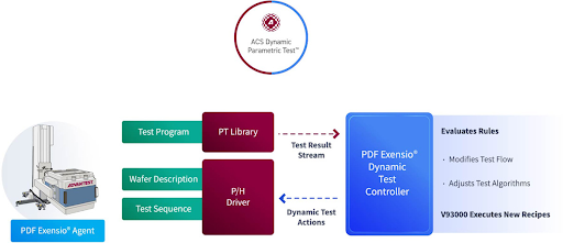
Advantest’s Dynamic Parametric Test (DPT) software is a data-analytics enhancement to the V93000 SMU8 parametric test system, built on PDF Exensio® software from PDF Solutions. Together, Advantest and PDF Solutions have built a focused solution for parametric test that programs human decisions and actions into the tester to add real-time intelligence into the parametric test cell. Users implement DPT to immediately apply modified testing, both test algorithms and die map topology, allowing them to gain greater insight into the causes of unexpected results and to improve the efficiency of the test cell.

Figure 2 illustrates how the two systems work together. The DPT solution includes modifications to both the V93000 SMU8 system software and the Exensio data analytics platform. The solution is integrated into the V93000 SMU8 and into the Exensio server that manages the rules engine. Using customer-created rules, the software evaluates the incoming data from the tester, determines any necessary modifications to the test flow and/or test algorithms, and communicates them back to the tester, which then executes the new recipe. All of this happens instantly, in real time.


Figure 2. The Advantest V93000 Dynamic Parametric Test (DPT) system powered by PDF Exensio® DPT. The V93000 measures data and, via the event data log (EDL) stream, sends it to the Exensio software, which evaluates the data and immediately transmits any adaptive actions back to the test system to run the revised recipe.

No pre-programmed instructions are included in the DPT solution. The customer defines rules and models based on their own historical data and manufacturing requirements, which the system uses to look for anomalies and automatically trigger appropriate actions as the tests are run. The system identifies three basic types of triggers:

  • A value that deviates from historical results;
  • A statistical computation based on historical results from wafers/lots/time; or
  • Statistical trends based on historical results from wafers/lots/time.

The rules that define these triggers and their parameters are set up through a simple user interface, using test algorithms already available in the customer’s test library, and are applied either at the end of the die location test or the end of the wafer test (see Figure 3).


Figure 3. The DPT solution can apply the rules engine at the end of a die-location test or at the end of a wafer test. New data in the modified test flow is automatically collected, without requiring wafer reloading or engineering review.

Real-world example

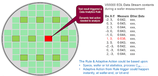
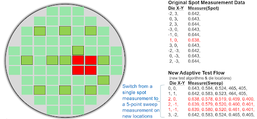
The ways in which the system can be deployed are limited only by customer needs. As an example, Figure 4 shows a use case involving diode test, checking the forward voltage (Vd) necessary for a 100nA of current to flow through the diode. The spot measurements are distributed across the wafer, as a representative sample provides a good indication of how the entire wafer behaves. When a bad data point is discovered, the system might automatically switch from a spot measurement to a sweep measurement, adding more die locations, to determine whether the cause is a device point defect or a general fabrication problem.

In Figure 4a, the DPT run flagged an outlier device that returned an out-of-spec result. As Figure 4b illustrates, this then automatically triggered a deeper, five-point sweep measurement around the location of the faulty diode, which revealed further outliers in that region. Figure 4c condenses the sweep results, plotting the sweeps to determine what caused the two parallel lines to appear. In this case, the slope shows normal diode behavior, with no device leakage. The problem is thus determined to be a problem with the bad diodes’ saturation current (Is).

The system’s further calculations reveal that Is is only modified by p-n junction area (via photolithography) or by dopant density in the anode or cathode. Knowing the potential contributors of the saturation current are physical area and impurity concentration leads to two different potential root-causes. The engineer can then look at the topological pattern, which, in this case, suggests that the problem was in either a photolithographic or etch step, likely from a single multi-die reticle exposure. Thus, in less than a second of automatic additional testing, DPT has provided the engineer with an augmented data set for quick problem resolution.

The system can detect virtually any type of problem created during the manufacturing process, including back-end probe testing. On most parametric test floors, continuity test failures due to failing probe contact are not uncommon. When a continuity test fails, DPT performs further tests to determine if the problem is actually a defective die location or a probe needle that needs to be cleaned or repaired.

Once DPT validates that previously good die are now failing, it automatically performs a wafer probe card clean/polish step. It then can explore a wider topological region, automatically adding die locations to determine where the continuity problem occurred. If the error was caused by a dirty probe needle, which is often the case, retesting the last failed die along with additional die nearby will confirm that the problem was fixed. Again, DPT saves time and money by cleaning probes at just the right time, prolonging their use, and preventing a pause in the fabrication process.

The future: intelligent DPT

As mentioned earlier, the ultimate goal of DPT is to utilize machine learning to make the process measurement results truly predictive, allowing parametric test to estimate wafers’ functional test yield as many days or weeks before they reach that step. With this type of forecast in hand, chipmakers could potentially alter the subsequent test plans and correct process deviations much sooner.

Looking again the manufacturing flow diagram, we see that, with the V93000-Exensio DPT solution, data becomes more valuable at each downstream step. As Figure 5 shows, the parametric test dataset can now be used to forecast functional test yield, days or weeks ahead of the wafers reaching functional probe test, accelerating reaction time to process anomalies.


Figure 5. Using DPT techniques feeds forward upstream manufacturing process data to optimize downstream testing.

The DPT solution is part of a broader manufacturing tool set that will provide greater value from data already being collecting or can automatically add to the dataset. In future versions, interconnecting data from wafer fab through package test will provide insights using other tools in the Advantest Cloud Solutions portfolio to accelerate manufacturing response time.

To learn more about the Advantest V93000/SMU8 + PDF Exensio Dynamic Parametric Test solution, plan to attend the 2021 International Virtual VOICE Developer Conference, June 21-23. For more information and to register, visit https://voice.advantest.com/

Read More

Posted in Q&A, Top Stories

Q&A Interview with Keith Schaub and Benjamin Lobmueller

By GO SEMI & Beyond staff

Advantest’s Grand Design sets goals for how the company will grow its business and markets over the next decade by integrating its solutions throughout the semiconductor value chain. Its cloud strategy is a vital aspect of this vision. To learn more, we talked with Keith Schaub, Vice President of Technology and Strategy, Advantest America, and Benjamin Lobmueller, New Business Development Manager, Advantest Europe. Their comments are aggregated below.

Q. What is the primary objective of your cloud strategy?

A. If you look at the semiconductor value chain [Figure 1], our core business, including our IC testers, handlers, and production processes, is in the middle. On the left-hand side, we’re mainly partnering with the EDA companies, and our focus is on design validation and verification. And on the right-hand side, we’re moving into system-level testing – this includes our acquisitions of Astronics’ System Level Test business (now ATS) and Essai, which added test sockets to our offerings. We’ve been working on these go-left and go-right strategies, as we call them, for several years. Now that those pieces are in place, we are focusing on our go-up strategy.


Figure 1. The cloud, AI and data analytics are the next steps in fulfilling the Advantest Grand Design.

For the most part, the data obtained from these processes and test cells is siloed. Customers use the data for their statistical techniques and yield improvements individually per process step, but none of it’s tied together cohesively. Our cloud strategy is to take all of these various process steps and use the cloud, AI and data analytics to connect them across the entire chain. Once you apply analytics and machine learning, you can predict the performance of future test insertions, to predict yields, outliers, even grades of performance, for instance. But this only works reliably if you have a system that spans the entire value chain.

These predictions then let you optimize what you’re going to do at a particular insertion based on information from the entire supply chain. If you know to expect good performance, you may need a less rigorous test. If performance is more marginal, rather than scrapping a device, perhaps you could perform additional testing that would allow it to become a tier-two device that would be viable to sell into a different market.

So, by tying all of these things together and applying AI and data analytics capabilities across the entire value chain, our customers and partners can optimize their insertions, whether for yield, quality, or cost. The systems can start to learn and improve over time. In a nutshell, that’s what this cloud approach is all about for us.

Q. How does this help make the customer’s job easier?

A. The hard part of what we’re trying to solve with this infrastructure is all the work you have to put in to get to the point where you can actually do analytics. Before you can analyze your data, many things have to happen, and what we’re doing with our cloud solutions is removing that burden from our customers.

For instance, if you have multiple insertions, you might have one process step in your supply chain in Taiwan and another one in Korea, while you are headquartered in Silicon Valley. How do you bridge that gap and bring together data from all those places? That’s where Advantest Cloud Solutions come in. We take away the tedious task of getting all your data in place so that you are better able to take advantage of real-time analytics, AI and machine learning techniques.

Q. What are some challenges of this approach?

A. Creating the infrastructure and getting all of these systems and customers to agree involves much cooperation. Everyone brings a separate piece to the table, and reaching consensus on the value can be challenging. So, while there are technical challenges, the business challenges are equal and sometimes even more significant.

We’re also taking away the difficulties from the information security side. Everyone has their security concerns – customers, OSATs, and us, of course – and those concerns need to be addressed. Advantest Cloud infrastructure is laying in all the necessary security nodes and layers, so that everything is protected appropriately.

Q. How do the new offerings fit into this strategy?

A. In December, as part of what we’re calling our Advantest Cloud Solutions [ACS] ecosystem, we announced Advantest Cloud powered by PDF Exensio, a data- and analytics-focused platform that we’re co-developing with PDF Solutions, as well as the ACS Dynamic Parametric Test powered by PDF Exensio.

This partnership came about when we decided to look at the best-in-class infrastructure pieces already available. In the process, we determined PDF Solutions to be the ideal partner. Their infrastructure is already in place with a large customer base. They have proven analytics tools that many customers use for decades, especially in the business’s foundry-side. With this partnership, they can continue to use those tools and expand to the industry’s test-side, and we can tie it in deeply to our infrastructure.

Our ACS products provide feedback on a wide range of processes, from semiconductor design validation to manufacturing, chip test, and system-level test – across all the different products and systems. This allows customers to get more value out of their supply chain, equipment, and test data, and get to yield faster. We can now give the customer a fully integrated infrastructure with analytics out of the box.

Q. How does all this work together to integrate the supply chain?

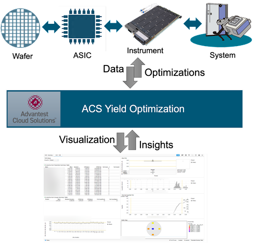
A. We’ve encapsulated that in Figure 2, which shows how the process steps work together with the Advantest Cloud as our corporate umbrella. It’s easy to say that we can just tie all these systems together, but these systems are not with one customer. They’re supplied by different customers of ours, working together for other customers of ours, in different geographies, and using different systems in many cases. For example, what format do you use to share the data? How do you protect the data as it moves from Customer A to Customer B? This illustration highlights what will be capable once all of this is in place.

Figure 2. Advantest Cloud Solutions deliver cross-supply-chain feed-forward/feedback capability.

It’s crucial to feed data forward in some cases, i.e., take data from a previous insertion to push it forward in the process and use that data in some intelligent way at a later stage. But it’s equally important to be able to have the data feed backward to improve your process. Say you find some problem at system-level test – it is invaluable to correlate back the possible causes so that you can predict the problem before it occurs in the future. Figure 2 is a graphical representation of different ways to feed data forward and backwards and what you would need to do that. The DEX network, which comes from PDF, has already solved many of the technological security challenges and includes measures to secure the data appropriately.

Q. Briefly, how does the ACS Dynamic Parametric Test product work?

A. The idea with ACS Dynamic Parametric Test powered by PDF Exensio is that we are essentially replicating product-engineering capability on the tester near real-time. What does that mean? What happens today is that a batch of wafers comes into a fab. They go onto a parametric tester. If there’s a problem, it’s typically assessed sometime later by an expert product engineer. This process carries a time cost – if something happens on a Thursday or Friday, it sits there over the weekend, and three or four days are lost. Meanwhile, the tester is booked for another job next week, so you have to deal with retesting everything and gathering the data.

The solution is ACS DPT, which utilizes the data analytics platform of PDF Exensio and uses a real-time rules engine to make decisions on the fly, while tests are conducted. So, when something starts to go awry with the measurements, the rules engine kicks in and flags it as a potential problem, taking extra data on all the nearest surrounding die. Once the test engineer looks at the situation, he or she has all of these additional bits of information to debug it. A much more intelligent decision can be made, much faster, and it can save millions of dollars when you consider multiple testers and multiple wafer lots.

Q. What else are you doing in the cloud?

A. We want to touch on a couple more things. The first is ACS Test Engineering Cloud, or ACS TE-Cloud, a service we’ve had for a while that we’ve now rolled up under our Advantest Cloud Solutions. It’s cloud-based test engineering that allows engineers to have an on-demand test program development environment. This capability is a game-changer, of course, for large companies, during a pandemic. Engineers can just keep working with the high performance they need, wherever they are. But it’s particularly beneficial for smaller players – new players in the market, for example, or startups or other ventures that need these tester services and don’t have a fleet of workstations to jump on. TE-Cloud gives them the environment to get the job done without investing millions of dollars in infrastructure that they may not need all the time.

With this service, we have flexible subscriptions available on demand. It’s very popular with our customers in China. They get remote access to our testers, we take care of all the hassles of infrastructure, and they don’t have to worry about calibration or maintenance. Again, many of these are tiny startups that can’t afford to buy a million-dollar machine just to get started. This way, they can get access to the test capability they need on demand.

The second thing we want to mention is Advantest Dojo, which we officially launched last summer. Dojo is our e-learning training environment in the cloud. Customers can get access to all training materials, videos and consulting, for different testers and services. It’s all being put under one umbrella to look and feel the same across geographies and the customer base. Customers pay a per-use fee to access this material, which application engineers within Advantest are continually updating to ensure the latest and greatest information is available.

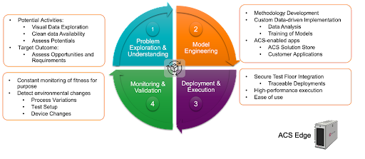
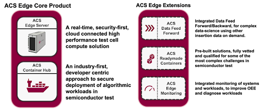
Finally, there is another new product, the ACS Edge high-performance computing system. There’s some confusion over cloud and edge, and why you need one versus the other. You do need both of them, and they have different use cases and value propositions.

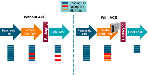
What the Edge means for us is that it’s right there at the test cell. The tester business model is that people pay by the second, so they want chips to go through as fast as possible. To make a prediction, you need to send data somewhere and get back an answer, as quickly as possible, about whether the part is good, bad or marginal. We optimize this with ACS Edge. It sits right next to the tester and plugs into the tester itself – the data streams directly over to it, and you get the lowest-latency HPC that you can get. You’re taking a supercomputer and plugging it into the tester so that you can make inferences with virtually no delay. You can think of it as bringing a data center to the test floor, or turning the test floor into a data center.

With ACS, we’re bringing both edge and cloud to the customer so that they can think up new use cases that employ data analytics and machine learning in both ultra-real time and post-insertion to get the predictive and high performance compute capabilities they need, most effectively, with the least impact on test cost.

Read More

Posted in Top Stories

ATE in the Age of Convergence and Exascale Computing

By Matthias Stahl, Business Development Manager, Advantest.

We are currently in the midst of the age of convergence – that is, the convergence of data from a range of applications and data sources. These sources constitute anything that creates data – ranging from human-created data, such as voice and video, through automotive, mobile, and wireless/IoT devices. This also includes edge computing and servers storing the massive amounts of data needed for high-performance computing (HPC), AI, machine learning and many other applications. 

This data must be processed, and that is where the age of convergence also becomes the age of exascale computing. The term refers to a supercomputer capable of calculating at least 1018 floating point operations per second. Currently, no single exascale computer exists, but the combined compute power available certainly exceeds this number. Figure 1 illustrates the parallels between data source and processing convergence that we are witnessing, with the chips and technologies that are being made for mobile, performance and next-generation computing – all of which have unique testing requirements.

Figure 1. The age of data convergence has given rise to the age of exascale computing

The V93000 platform has been used successfully for HPC test since its introduction in 1999. It became part of Advantest with the acquisition of Verigy in 2011, and we’ve continually added new capabilities that have enabled us to keep pace with customers’ HPC needs. Figure 2 shows that many diverse drivers are creating the need for these new capabilities.

Figure 2. Exascale computing creates new ATE requirements.

As transistor count increases with smaller nodes, scan data volume goes up as well. This creates the need for deeper memory, faster scan, and new methodologies. At the same time, as device nodes continue to shrink, power-supply requirements escalate – not just power as such but also power dynamics. For example, devices require power supplies that can accommodate fast switching with no glitches, providing stable and consistent performance.

Concurrently, multisite testing demand will increase, with the industry looking to keep test costs in line. Another trend is the integration of RF capabilities into many devices, requiring a test platform that can accommodate the full range of RF and digital test. Today, we already have power management ICs (PMICs) close to the CPU, and we will see more uses going forward for data center applications, creating high-voltage test requirements. 

Bringing test into the exascale age

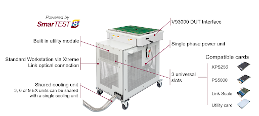
The new EXA Scale™ Generation of the V93000 (Figure 3) addresses these challenges with advancements to the proven V93000 architecture, designed to enable new test methodologies. Initially targeted at advanced digital ICs up to the exascale performance class and RF devices, more applications like MCU or automotive device test will be added. The system is designed to provide superior processing power for massive test data, as well as the highest possible currents and up to 256 power channels per card. The tester and handler can be tightly integrated, which, when combined with the tester’s active thermal control, allows the test cell to offer superior thermal control overall. 


Figure 3. The V93000 EXA Scale features powerful processing capabilities in a compact footprint.

Four key innovations enable the newest V93000 tester to deliver exascale-level performance: Xtreme Link; new test heads; and a new universal digital and power supply card (Pin Scale 5000 and DC Scale XPS256 DPS, respectively) for lower cost of test and faster time to market.

Xtreme Link

The V93000 EXA Scale incorporates Xtreme Link, our specialized ATE network with edge computing capabilities. Rather than using off-the-shelf technology like Gigabit Ethernet, we created dedicated technology with an optimized protocol focused on test needs and requirements for high throughput and large test data handling. Figure 4 illustrates the structure and benefits of this network.

Figure 4. Xtreme Link technology enables massive scalability and flexibility for the V39000 EXA Scale.

Pin Scale 5000

The Pin Scale 5000 is a new digital instrument created to set a new ATE standard for scan test. The fastest general-purpose ATE pin on the market, it offers 256 pins running at 5000Mbps maximum speed, scan result capture at up to 5000Mbps, and <1.5ps RMS jitter for accurate reference clocks. The Pin Scale 5000 also features the deepest vector memory available, with 3.5G gigavector (GVec) scan per pin, or 28GVec scan per 8 pins using pooling and fan-out technology. It’s designed to enable all scan implementations, including parallel, multiplexed and HSIO scan, and its configuration flexibility supports high site count – this allows customers to speed their overall test time by performing parallel core test. 

Figures 5 and 6 provide examples of the superior measurement and performance capabilities that the card enables.

Figure 5. Pin Scale 5000 phase noise measurement example. The RMS jitter is just 0.9ps, well below the specified 1.5ps.

Figure 6. Pin Scale 5000 receiver performance at 5Gbit differential. Even at top speed still 55% height and 75% width.  

DC Scale XPS256

The XPS256 combines the best capabilities of several predecessor Advantest instruments. It features many pins with small currents (256 pins x 1A), and it can gang those resources to achieve high current as needed. Combining these capabilities in one DPS allows the XPS256 to offer optimal flexibility and utilization of resources, in a common configuration well suited for 5G, mobile and HPC/AI applications. In addition, its improved accuracy and dynamic response enable achievement of higher yields.

The XPS256 power supply covers wide-ranging current requirements, implementing unlimited ganging to scale from milliamps (mA) to thousands of Amps with no performance degradation. Combining three instruments in a single power supply, the DPS pin delivers best-in-class flexibility, accuracy (±150µV) and dynamic response, with full four-quadrant voltage-current (VI) capabilities and very small overshoot/undershoot, and provides zero-overhead simultaneous voltage and current monitoring. 

A unique feature of the XPS256 is its built-in probe needle protection. With individual needles connected to separate power supply pins, currents can be limited to 1A or less per needle. An ultra-fast (<1 µs) hardware clamp allows current to be limited and shut down almost immediately if needed.

Both the Pin Scale 5000 and the XPS256 utilize Advantest’s unique next-generation multicore test processor. The processor is packaged using 2.5D integration, with two 8 core die, and two memory chips, providing 16 fully independent pins in a very small form factor.


Figure 7.  Test processor and memory for 16 channels. 

New test heads

Three new extended test heads developed for the EXA Scale generation tester offer superior configuration scaling from engineering to high multisite applications: the V93000-CX with 9 universal slots, the V93000-SX with 18 universal slots, and the V93000-LX with 27 universal slots. All feature a “zero footprint” design – all electronics are integrated into the test head, eliminating the need for a separate rack. Together, the new test heads cover all application segments and a wide price range, while their enhanced infrastructure helps contribute to lower cost of ownership for customers.

Platform compatibility facilitates transition

The EXA Scale generation of the V93000 platform is compatible with the Smart Scale generation. Smart Scale cards will work with EXA Scale, the load board dimensions are compatible for ease of migration between the systems, and the EXA Scale system can run both the SmarTest 7 and SmarTest 8 versions of our ATE programming environment. This will allow customers the ability to select the V93000 configuration that best meets their product and application requirements.

To date, we have already shipped a significant number of V93000 EXA Scale systems, both for engineering and high-volume production, to multiple customers. We look forward to sharing further successes as the age of exascale computing speeds forward.

Read More