Pages Menu
TwitterRSSFacebook
Categories Menu

Posted in Top Stories

Design Considerations for Ultra-High Current Power Delivery Networks

This article is adapted from a presentation at TestConX, March 5-8, 2023, Mesa, AZ.

By Quaid Joher Furniturewala, Global SI/PI Manager, R&D Altanova, Advantest

A power-delivery network (PDN), also called a power-distribution network, is a localized network that delivers power from voltage-regulator modules (VRMs) throughout a load board to the package’s chip pads or wafer’s die pads. The PDN includes the VRM itself, all bulk and localized capacitance, board vias, planes and traces, solder balls, and other interconnects up to the device under test. An optimized power-delivery approach will employ a decoupling scheme that provides low impedance to ensure a clean power supply. An optimized PDN will result in more power being transferred from the VRM to the DUT, with supply voltage held constant within a narrow tolerance band with minimal ripple under load.

PDN optimization is becoming increasingly important as more and more high-current applications appear. Keep in mind that power equals I2R, so even a slight amount of load-board resistance imposes significant power dissipation at high currents. For a 2.5-kW device, a 5% drop in power is 125 W! Table 1 shows how device voltage and current and load-board dissipation are trending over time.

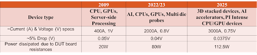
Table 1. Device-power and load-board-dissipation trends

PDN optimization

For effective PDN optimization, prioritize the supplies, keeping in mind that not every supply can be optimized to achieve tight margins, and tradeoffs may be required. Also, plan your DUT board stacking based on power dissipation (Figure 1), and note that usually, the DUT vias account for the highest inductances in the PDN path. Plane inductance is negligible compared with via inductances.

As the industry moves to devices with high current demands, the historical rules of thumb and reference guidelines are no longer adequate. Following antiquated rules can lead to poor hardware design, requiring costly re-spins, dropped yields, and lost time. A proper PDN needs to be designed based on the device specifications to ensure a good power delivery network.

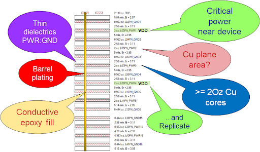
Figure 1. Plan your DUT board stacking to keep critical power near the device.

You can follow several recommendations when optimizing your load-board layout:

  • Move or replicate critical power close to the DUT to reduce via impedance.
  • Increase capacitor via size and use multiple vias at all capacitor pads.
  • Put high-speed capacitors on the top side of the board.
  • Use low equivalent series inductance (ESL) capacitors.
  • Increase DUT via size to the extent permitted by your design-for-manufacturing (DFM) rules.

Contrary to popular belief, the under DUT capacitance (capacitor placed on the opposite side of the device on power vias) is not always effective. The capacitance may be dominated by the inductances of the long and thin DUT vias. Consideration needs to be given when choosing the value of the capacitance under the DUT. The least inductive way to effectively utilize decoupling would be to route the power closer to the device so that the DUT vias are short and place decoupling on the top side very close to the DUT with bigger vias.

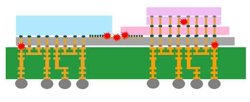
When it comes to having the power delivered to the DUT with the least electrical resistance, offsetting the DUT vias towards the corner of the device to create a channel for current to flow to the device core can be a good strategy (Figure 2). If your DUT has high-speed pins or channels on a few quadrants, the others can still be offset to create a channel for the current to flow.

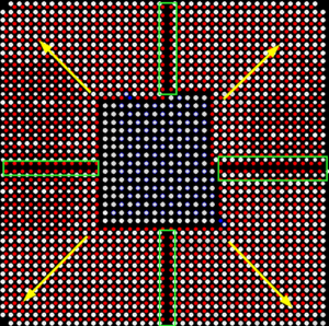
Figure 2. Offsetting the DUT vias toward the corner of the device can be a good strategy.

As the PDN return path on most ATE designs is shared with signal lines, the return path shares the return currents for the signal and power. Consequently, the return path becomes a non-trivial consideration. If the design has shared signal and power lines, the return path needs to be wide enough to ensure the current does not get constricted and create ground-bounce issues.

If the layer stacking allows for a GND-PWR-GND type structure, it is always recommended due to the noise coupling isolation and better power impedance. However, this is not practically possible in very dense and high site count designs where the thickness of the circuit board is limited due to the aspect ratio concerns with the fabrication of the board (aspect ratio is the ratio of the drill size to the board thickness). In this case, the GND-PWR-PWR-GND approach can be used (Table 2). It will offer slightly poor noise isolation but can be used for low-current and less noisy supplies, while GND-PWR-GND can be used for high-current supplies. 


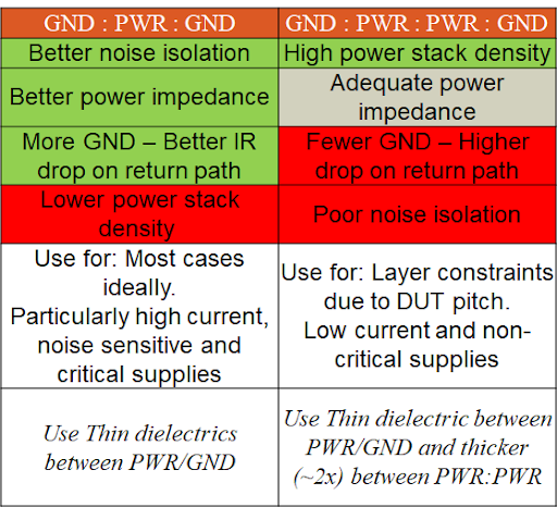
Table 2. Return-path considerations

PDN power-integrity (PI) analysis is a key to delivering ripple-free, low-noise, stable voltage to the device pads. PI analysis begins with a pre-layout analysis on all the power rails with the definition of your target impedance and decoupling strategy. Post-layout analysis is done after decoupling capacitance is placed and power is routed. Post-layout analysis includes all the PDN elements from VRM to DUT, and it involves DC, AC, and sometimes thermal analysis.

DC analysis
DC analysis examines via currents, current density, and voltage drop, including return-path voltage drop, due to resistances in the board current path. DC analysis helps identify bottlenecks due to copper depletion. Performance can generally be improved by increasing the copper area, replicating power planes, and increasing copper weights on stacks.

A case study involving a 2.4-kW device provides an example of DC analysis. The package includes a channel to provide better current flow near the core. The load board includes 2-oz copper layers with multiple high-current supply layers. A 1-mm pitch allows larger 14.5-mil power and return vias. Power shapes added in the signal layers based on available space help to improve performance. Table 3 shows IR drop simulation results for the various supplies. Total power dissipation is 83 W or less than 3.5% of the device’s 2.4-kW rating


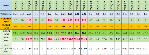
Table 3. DC analysis of load board for 2.4-kW device

AC analysis

AC analysis is the study to understand how the load ripples at varying frequencies. It is analyzed using impedance vs. frequency plots to determine whether the decoupling strategy is sufficient to meet the target impedance for the supplies.

At DC to the lower frequency ranges (<10 kHz), the region of lowest impedance on the ATE board is the ATE power supply region, and the path of least resistance is through the DUT power and return planes. As the frequency gets higher, the path of least resistance is through the bulk capacitors, high-frequency capacitors, and finally, the on chip capacitors, respectively. Capacitance on the PDN is designed to cover the entire device-clock-frequency spectrum in order to eliminate the voltage ripple generated by the device’s switching currents.

Each power rail requires a power-supply target impedance ZT as a function of voltage VDD, percent ripple, and transient current:

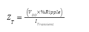
The target impedance calculations need to factor in the maximum ripple voltage that the DUT can tolerate (for example, 5% of VDD). It must also factor in maximum transient current, which is not always known. As a rule of thumb, ITransient is 50% of IMAX.

As an example, for a 10-A, 7.5-V VDD supply, a 5% ripple spec, and ITransient that is 50% of IMAX, the target impedance is 7.5 mΩ

When determining target impedance, keep in mind that keeping impedance much lower than necessary will result in an overdesigned PDN and unnecessary cost.

Thermal analysis

Finally, thermal analysis involves studying temperature rise in circuit-board structures as currents increase. An effective strategy for thermal analysis is to employ PI-thermal co-simulation, which calculates heat generated as current flows through the metal structures of a load board from the VRM to the DUT.

Thermal analysis must consider the current flow from all supply rails but take into account the fact that not all supplies are necessarily activated at the same time. PI-thermal co-simulation is particularly useful for very high-power designs to identify hot spots that could cause damage to the board or DUT.

Thermal vias spread throughout the board with copper ground-flooding on the outer layers can minimize thermal problems. So can any additional structures, including frames and stiffeners, as they also act as heatsinks.

Figure 3 shows a thermal analysis that confirms satisfactory board temperatures resulting from supply currents. Supplies were run individually and in combinations of multiple supplies with a common return path. This simulation did not consider heat generated by components or the DUT itself.

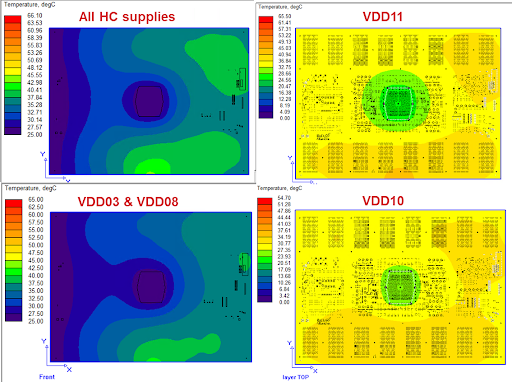
Figure 3. This thermal simulation shows heat generated by currents from individual supplies and combinations of supplies.

No matter how careful the design, thermal problems can appear during normal load-board operations. You can consider adding temperature sensors such as the Sensirion SHT35 and Texas Instruments TMP1075 to the board, placing multiple sensors on top and bottom sides in different locations. The sensors can communicate over an I2C interface and send an alert signal to the tester, which can be read on the tester pin-electronics channels when a temperature threshold is exceeded to perform a supply shutdown when needed.

Thin-core dielectrics and thick stacks

Other considerations in load-board design include the use of thin-core dielectrics and thicker stacks. Thin cores, such as 12-µm cores, are useful for printed-circuit-board power and ground structures. They permit higher layer density and lower plane inductances, offering impedance reductions of 10% to 45% compared to normal-thickness dielectrics (Figure 4). Note, however, that they are more costly, present handling risks, and may be hard to source.

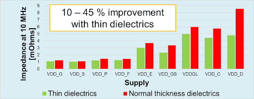
Figure 4. Thin dielectrics can provide a 10% to 45% improvement compared to normal-thickness dielectrics.

As for thicker stacks, existing ATE fabs offer board thicknesses up to 0.330 in. with a single lamination. Advanced fabs can create boards with thicknesses up to 0.400 in., increasing layer density by 21% (Figure 5). Thicker, higher-density stacks enable more layers for power planes. They are useful for CPU, GPU, and AI accelerator ATE boards, as well as memory probe and other probe tests. In addition, they support an increased number of layers with 2-oz copper cores to help improve PDN performance. R&D Altanova is in production of such boards effective this quarter.

Figure 5. Thicker, higher-density stacks can help improve PDN performance.

Conclusion

PDN performance is critical for the design of load boards for today’s high-current devices. Thermal concerns are increasingly significant as DUT power ratings increase. Design optimization and proper PDN power-integrity analysis will ensure that the power delivery is good without any power stability issues, thus increasing the yields for device under test. It will ensure a good working hardware and save precious time and cost for the board re-spins.

Read More

Posted in Top Stories

Comparison of State-of-the-Art Models for Socket Pin Defect Detection

This article is adapted from a presentation at TestConX, March 5-8, 2023, Mesa, AZ, by Vijayakumar Thangamariappan, Nidhi Agrawal, Jason Kim, Constantinos Xanthopoulos, Ira Leventhal, and Ken Butler, Advantest America Inc., and Joe Xiao, Essai, Advantest Group.

By Vijayakumar Thangamariappan, R&D Engineer, Expert, Advantest America Inc.

Test sockets have a key role to play in the semiconductor test industry. A socket serves as the critical interface between a tester and device under test (DUT). Although seemingly simple in concept, a socket can have thousands of pins, depending on the number of I/O connections to the target device. A typical socket size might be 150mm x 200mm x 25mm, and protruding pin height may be about 50 to 250 micron (Figure 1). Manufacturers may produce thousands of sockets per month or more, and each pin of each socket must be inspected so that pin defects do not impact semiconductor production test and cause expensive downtime.

Figure 1. A socket (top) may include thousands of pins, shown back (bottom left) and front (bottom right).

During socket assembly, several problems can arise. Too much pressure may be applied, one or more holes may be skipped, a pin meant for one hole may be inserted in another, or foreign material may contaminate a pin location. Figure 2 shows several defect types, including apparent pin defects caused by image capture errors.

Figure 2. Pins can exhibit several defects, some of which may be artifacts of the imaging system.

Traditionally, an inspection engineer has used a microscope to identify pin defects. But even for a highly trained engineer, the process is highly subjective, time-consuming and error-prone. The manual approach makes it particularly difficult to identify mixed-pin issues, which occur when a pin meant for one hole is inserted into another, and wrong pin issues, which occur when a pin meant for one socket type is inserted into another (Figure 3).

Figure 3. Manual inspection makes identifying mixed-pin (left) and wrong-pin (right) issues difficult.

In addition, manual inspection is difficult to scale for high-volume manufacturing. In general, it can lead to test escapes, reducing customer satisfaction, functionality, reliability, efficiency and productivity. A single pin failure can lead to system application failure or damage to the DUT, and a defect found at a customer site would require tester downtime to troubleshoot. Once the defective pin is identified, the socket assembly will require rework and retest, negatively impacting production throughput and imposing shipping delays.

Automating the inspection process

Consequently, it becomes desirable to automate the inspection process by applying artificial intelligence and machine learning. The first step involves considering concepts such as object classification and object detection. Object classification returns the class of an object, such as “cat” (Figure 4, left). Object classification provides no localization information regarding the position of the object—it merely indicates whether an object of a particular class, such as “cat,” is or is not present. In contrast, object detection identifies the classes of objects in an image (for example, “dog” and “cat” in Figure 4, right) and surrounds them with bounding boxes (green and red rectangles in Figure 4, right) to indicate their locations.

Figure 4. Object classification can identify the class of an object in an image (left), while object detection identifies object classes and locates them within bounding boxes (right).

For socket pin-defect inspection, object detection is the preferred approach. For object classification, limited interpretability (that is, distinguishing the class of “good pins” from the class of “defective pins”) makes identifying corrective actions difficult, and background variability (such as socket surface patterns) greatly affects results. In contrast, object detection can help identify and locate different object types, with background variability ignored.

Having decided on object detection, we evaluated three object-detection algorithms:

  • YOLO (You Only Look Once) employs a one-step process that performs classification and established bounding boxes at the same time.
  • Faster R-CNN (Faster Regions with Convolutional Neural Networks) employs a two-step process providing, first, a region proposal, and second, object detection within the proposed region.
  • SSD (Single Shot Detector) employs a one-step process that divides an image into a grid to locate objects within the image.

Training these algorithms requires many images for every class of object of interest. Because the pin defect rate in a manufacturing line is low and some defect types are rare, it is difficult to select a balanced dataset. Our approach was to group all defective pins under a single class named “defective.” We then defined two additional classes, “big pin” and “small pin,” to train a single three-class model. Each pin image has a size of 792 by 792 pixels. 

Figure 5 shows our training and validation dataset on the left and the number of defect types that make up our “defective” class on the right.


Figure 5. The defective class in the training dataset (left) includes jammed pin, missing pin, foreign material (FM), bent pin, image capture error (ICE) and wrong pin defects (right).

We next employed the semiautomated bounding box preparation process outlined in Figure 6.

Figure 6. Bounding box preparation requires a five-step process.

The steps are as follows:

  1. Apply Gaussian blur
  2. Find a mean value and reset all pixel values to white if the pixel values are greater than the mean
  3. Do a binary invert
  4. Find max area contours
  5. Draw the bounding box

Figure 7 outlines the confusion matrix of possible outcomes. False positives imply test escapes, while false negatives require more time to evaluate bad images.

Figure 7. In this confusion matrix, false positives imply test escapes and false negatives require more time to investigate.

To evaluate algorithm performance, we focused on time and accuracy as key metrics. Speed is crucial because the model will be deployed in a post-assembly socket manufacturing line. In addition, high-volume manufacturing generates a large amount of input data, so a model that can predict an object class quickly is necessary. Accuracy is necessary to minimize false negatives and prevent test escapes.

To measure the inference time of all three models, we deployed them on Amazon EC2 instances, which are commonly used to host machine-learning models used in image classification and object detection. We chose instance type g4dn.16xlarge, which has an NVIDIA Tesla T4 16-GB GPU. Table 1 shows the results.

Table 1. Model Inference Time

The Faster R-CNN algorithm required the longest processing time, as expected, because it has a two-layer network architecture. YOLO and SSD have single-layer architectures and had shorter inference times, with YOLO outperforming the other two.

Our results show that YOLO also outperformed the other two algorithms in terms of accuracy.  Accuracy metrics primarily focus on false positive (test escape) and false negative (need review) results. YOLO misclassified only five good pins as bad pins (false negative). The low false negative count drastically simplified the post prediction review process. The following list summarizes our observations regarding the test escapes:


  1. Test escapes: All models performed well in identifying jammed pin, bent pin, and wrong pin defects. YOLO correctly identified all missing pin defects, while Faster R-CNN and SSD had eleven and two misclassifications, respectively. Both R-CNN and SSD had test escapes. 
  2. Conditional test escapes: YOLO outperformed the other two models in identifying foreign material and image capture error classes. YOLO’s 10 false positives are from seven foreign-material (FM) defects and three image-capturing errors (ICEs).
    1. FMs that clog the whole pin region are the real problem. Compared to other models, YOLO’s seven FM misclassifications resulted from either a tiny FM particle in the pin region or FM that did not affect pin hole region. We recommended additional cleaning procedures before inspection to avoid this issue. 
    2. An ICE is an issue caused by the image-capture equipment. ICEs do not represent actual pin defects but do result in noise being added to the image.  In YOLO’s three misclassified image-capturing errors, pin regions are clearly visible, and the issue occurs outside the pinhole region. We took additional measures to avoid these randomly generated ICE issues. Table 2 summarizes our overall results.


Table 2. Model comparison with metrics

Advantest ACS Edge solution

As mentioned, we performed our model evaluations in an Amazon AWS cloud environment. To achieve faster prediction speeds in an actual manufacturing facility, you can forego the cloud-service hosting and instead use Advantest ACS EdgeTM.  It is a highly secure edge compute and analytics solution which can host computationally intensive workloads adjacent to the test equipment. The Advantest ACS Edge solution provides consistent and reliably low latencies compared to datacenter-hosted alternatives.

Figure 8. ACS Edge can host models with low latency.

Conclusion

The primary goal of socket pin-defect detection is to reduce the need for manual inspection while maintaining zero test escapes. We compared three different object-detection algorithms to find the best combination of accuracy and processing speed. The YOLO model was able to learn pin-type features quickly, achieving higher accuracy with fewer iterations compared with the other models.

Read More

Posted in Top Stories

Device Validation: The Ultimate Test Frontier

This article is a condensed version of an article that appeared in the November/December 2022 issue of Chip Scale Review. Adapted with permission. Read the original article at https://chipscalereview.com/wp-content/uploads/flipbook/30/book.html, p. 26.

By Dave Armstrong, Principal Test Strategist, Advantest America

In the early days of space exploration, spacecraft were manned by small teams of astronauts, most of whom were experienced test pilots who intimately understood their vehicles and the interaction between all the variables controlling the craft. Similarly, early integrated circuits (ICs) were created by small teams of engineers, who often designed, laid out, and even developed tests for their devices. Notably, the tests were most often functional, and the test interfaces were often analog. Over the years, ICs have become much more complicated, and team size and group effort have grown exponentially. Today, the fundamental limitation to continued industry growth is no longer gate length, but team size and strength.

Contending with unconstrained growth to test data volume, as well as effort, requires a vision for taming this growth in the not-too-distant future. That vision must focus on intelligent applications, first-silicon “bring-up,” post-silicon validation (PSV) test, and production test. The challenge, paraphrasing Star Trek, is to boldly go where no test solution has gone before.

This article describes four different validation and test methods and how their values and focus have shifted over time, then discusses the limited growth of tools and methodologies in functional testing and PSV. Going forward, by leveraging such established best practices as standard interfaces, automation, and scalability, we will be able to streamline first silicon bring-up.

Method 1: Device validation/characterization

Early device testing and functional validation typically involved five elements:

  1. Instruments connected to primary device inputs and outputs;
  2. Instruments to program the device into its various modes of operation and environmental extremes;
  3. Wires to interconnect instruments, the device under test (DUT), and a test-system controller;
  4. An intelligent operator who controlled the setup to pinpoint problems and determine optional operations; and
  5. A test controller program typically coded in some proprietary test scripts.

Over the years, the increasing complexity of devices and relentless time to market (TTM) pressure resulted in a need for multiple setups enabling concurrent engineering. Note that experts will still need their functional test setups when called upon again to help with yield investigations and field returns.

Method 2: Functional test at ATE

The first automatic test equipment (ATE) tests were all functional. Some argue that the most valuable ATE-based tests are still functional. These tests on the ATE use a few well-understood instruments interconnected through a tightly controlled device under test (DUT) interface to confirm to the extent possible the proper operation of the device in mission mode. Functional tests on ATE are typically analog, measuring parameters such as Vmin and Fmax over temperature extremes. What ATE functional test cannot do is run tests that require attached memory, peripherals, or both. This lack of full-functional test coverage has driven the recent rise in the use of system-level test (SLT), discussed in Method 4.

Method 3: Structural test

As ICs became more digital, scan chains provided a standard way to access the innards of the DUT, and automatic test pattern generators (ATPGs) addressed the tedious pattern-generation challenges. The use of ATPGs was highly successful over the years because it:

  • Was automatic;
  • Provided a testability baseline that defined a minimum acceptable quality level;
  • Leveraged a consistent DUT interface that then drove consistent instrument interfaces;
  • Worked well in a distributed engineering environment; and
  • Allowed test costs to scale slower than Moore’s Law, thanks to enhancements such as pattern compression and homogeneous-core pattern sharing.

As device complexities grew, so did the test data volume needed to traverse the logic and confirm proper logic cell operation. The International Technology Roadmap for Semiconductors (ITRS), which tracked this ever-increasing data volume, showed years ago that the structural test generation effort was growing even faster than Moore’s Law. As the levels of logic grow deeper and deeper, it takes more and more vectors to gain the controllability and observability necessary to effectively test the part.

One significant limitation of structural testing, which necessitated the growth of SLT and the continued utilization of functional validation efforts, was the ever-growing list of fault types for structural testing to target. Moreover, the trend toward More-than-Moore multi-die integrations brings together multiple devices and exacerbates the testing challenges.

Method 4: System-level test

For years, SLT has provided value by checking that a device can operate in its end-application mode (for example, that it can boot an operating system and run representative end-user applications). Because its tests occur later in the flow, it catches more problems at the edge of the various cores and/or devices (that is, interface faults). A clean consistent setup that supports the device while maintaining the visibility needed to catch faults is key to a visible SLT hardware setup. For devices with on-die processors, recent efforts have graduated beyond running power-up routines to running automatically generated code sequences, which both utilize and confirm the ability of the embedded processor to sequence through tests while performing their duties.

Test moving into the 21st century

Device validation/characterization, functional test at ATE, structural test, and SLT will continue to find use in the 21st century. But just as Star Trek had the next generation, so, too, must test. The next generation of test clearly needs to be smarter and leaner. Moving forward, the role of data and artificial intelligence (AI)-driven smart tools (Figure 1, in purple) will become more pronounced, allowing tests to be streamlined and risks reduced.

Another significant change is the prospect of using data from other sources (Figure 1, in light blue), both to focus the tests on areas of concern and to adjust the test margins to reduce the risk of shipping a bad part—all while minimizing the cost of test. ATE’s instruments and capabilities can contribute in the ways shown below; the newest are in italics.

    1. Expanded wafer testing (first view of new wafers)
    2. Known-good-die (KGD) test (at-speed and at-temperature testing at the wafer or singulated-die level)
    3. Enhanced first-silicon testing (device validation, driver development, and checkout)
    4. Final test (at-speed and at-temperature testing after packaging)
    5. System-like test™ (Advantest’s term for focused system testing on ATE)
    6. Post-silicon validation (including parameter/register value optimization)
    7. RMA testing (i.e., testing of field returns)

Figure 1. Multiple tools, including PSV and ATE, are used for device checkout.

Pre-silicon validation 

Prior to the arrival of first silicon, design verification involves running test cases in a simulator or emulator at great length. The incredible growth in device complexity has greatly increased the effort and time it takes to verify a design before its tape-out. To increase engineering productivity, test development must be supported by standardized methodologies and tools. The latest standard enabling system-level modeling and test design is the Portable Test and Stimulus Standard (PSS), developed by Accelera. PSS is supported by major electronic design automation tools and significantly increases test quality and shortens time to market (TTM) through improved productivity in design verification.

The need for the Industry to “shift left” has been explored in other works [1,2]. Just as some test content must shift to wafer-level testing, so, too, the preferred path to improve TTM and reduce the likelihood of a re-spin is to shift wafer test content further to the left and expand validation efforts prior to first-silicon arrival. That said, pre-silicon validation has limitations, e.g., abstract, higher-level models (such as virtual prototypes) may not provide an accurate estimate of the power consumption or Fmax for given code snippets. Optimizing the test content and value of each step in the process is a key challenge in the 21st century.

First-silicon bring-up

While there is real value in running scan-based structural tests, unfortunately, history has shown that these tests are not nearly enough to confirm that a device is truly functional. Leveraging today’s multi-week assembly cycles, significant value can be achieved by running some mission-mode functional tests at wafer probe. By migrating functional test content to the wafer level, companies have saved multiple weeks of TTM during their device turn-on phase [3]. One approach toward migrating test content to an earlier test step is to use Advantest’s Link Scale™ digital channel cards for the V93000 platform (Figure 2). LinkScale cards enable software-based functional testing using USB or PCIe, in addition to scan testing of advanced semiconductors, and address testing challenges that require these interfaces to run in full protocol mode, adding system-like test capabilities to the V93000.

Figure 2. Continuous validation and testing add TTM value.

LinkScale has proven its value in first-silicon situations by providing a straightforward path for R&D engineers to quickly perform traditional functional test verification steps after the arrival of first silicon. Early verification moves forward the clock for confirming truly good devices, but also speeds identifying problems and workarounds should they be needed. Perhaps the most important value of this approach is in the resource requirements. The new solution provides a quick and easy path enabling R&D engineers to gain full access to their design, highlighting subtleties that were difficult or impossible to discern using pre-silicon validation techniques. Furthermore, engineers can explore operational corner cases whose impact was never fully communicated or understood—all within days of first silicon arrival!

Post-silicon validation (PSV) 

Because of the limitations of pre-silicon validation, the design engineer is often called upon to tune power and high-frequency performance soon after first silicon arrives. This tuning requires an effective flow to bring up a comprehensive set of PSV tests that support flexible parameterization. Without comprehensive PSV that identifies marginalities, an end product may behave erroneously under certain environmental conditions and loading. The industry experiences this in many ways—one example is “silent data corruption” in data centers when devices deliver wrong results under particular circumstances. 

Advantest’s EXA Scale EX Test Station simplifies or can replace yesteryear’s bench setup. It provides for a clean and consistent workspace that also happens to be identical to the setup used in production testing on the V93000 ATE. The test station supports both functional and structural test content execution, allowing the PSV engineer to move seamlessly between the two domains to confirm the root cause of incorrect behavior. The addition of structural test capabilities to the bench environment enables the test engineer to step into or over problematic sections of the test to enhance visibility and control.

Another new capability in the PSV effort is software-driven functional test, in which software test sequences provide input to the functional test-generation effort (Figure 3). The EX Test Station, together with creative software tools, allows broad ranges of register settings to be explored automatically to pinpoint the best possible operating condition with less human effort.

Figure 3. Software-derived tests enable LinkScale to check that real-world code works on real-world hardware.

Production test

Nearly all test content needs to move to the wafer test step if we are to have any chance of achieving KGD. We have entered a space where we have too many tests and not enough time to run all of them. Manufacturers today typically cull about 10-50% of their available pattern sets at wafer probe because of vector-memory and/or test time limitations. The question moving forward is how to choose which patterns to run at each test insertion point. Today, this is an art left to the senior test strategists; moving forward, this art will benefit from AI-driven tools and broad-based data sharing.

The big opportunity for growth in this space is with the addition of data-driven test selection techniques that allow both the structural and functional test selection process to proceed more intelligently. To proceed, actions to consider include:

  • Pulling in and using vision inspection data to decide which corner of the die to test first;
  • Using in-line parametric test data to anticipate power extremes and appropriately adjust limits up front; and
  • Using the results for the first few wafers to direct which tests should be executed subsequently.

Summary

As we move into 21st-century test, things will become much more focused and dynamic. There is little doubt that data will be king. There is no doubt that test over HSIO interfaces will become critical to test time reductions. And perhaps most important, the role of big data in determining the value and limitations of each device being tested will be solidified.

The EXA Scale EX Test Station (Figure 4) replaces multiple instruments and tangles of wire with a streamlined integrated system and provides for a clean and consistent workspace. A consistent interface achieves consistent results.

Figure 4. The old way of validating designs (a) is superseded by the Advantest EXA Scale EX Test Station (b), shown docked to the M4171 remotely controlled high-powered handler

Given that the role of data in the future will continue to expand and grow, it’s quite prophetic that Star Trek: The Next Generation had a robot named Data who gave voice to the challenge we face: “It is the struggle itself which is most important. We must strive to be more than we are. It does not matter that we will never meet our ultimate goal. The effort yields its own rewards [4].”

References

  1. D. Armstrong, “Shift left,” MEPTEC Known-Good Die Workshop, Sept. 25, 2022, https://www.youtube.com/ watch?v=YObxvk5sqSQ&t=241s
  2. D. Armstrong, “Heterogeneous integration prompts test content to ‘shift left,’” Chip Scale Review, Feb. 2021, p. 7. https://chipscalereview.com/wp-content/uploads/flipbook/1/book.html
  3. B. Tully and M. Kozma, “Advantest’s new Link Scale card for SCAN, functional, mission mode SLT and validation testing,” VOICE 2022  
  4. “69 Best Data Quotes from Star Trek TNG and the Star Trek Movies,” Soda and Telepaths, April 26, 2021. https://sodaandtelepaths.com/69-data-quotes-from-star-trek-tng/


Read More

Posted in Top Stories

Data Analytics for the Chiplet Era

This article is based on a paper presented at SEMICON Japan 2022.

By Shinji Hioki, Strategic Business Development Director, Advantest America

Moore’s Law has provided the semiconductor industry’s marching orders for device advancement over the past five decades. Chipmakers were successful in continually finding ways to shrink the transistor, which enabled fitting more circuits into a smaller space while keeping costs down. Today, however, Moore’s Law is slowing as costs increase and traditional MOS transistor scaling have reached its practical limits.

The continued pursuit of deep-submicron feature sizes (5nm and smaller) requires investment in costly extreme-ultraviolet (EUV) lithography systems, which only the largest chip manufacturers can afford. Aside from lithography scaling, approaches for extending Moore’s Law include 3D stacking of transistors; backside power delivery, which moves power and ground to the back of the wafer, eliminating the need to share interconnect spaces between signal and power/ground lines on the wafer frontside; and heterogeneous integration via 2.5D/3D packaging with the fast-growing chiplets. All these new constructs have been formulated to enable the integration of more content into the package.

With these new approaches come heightened package density and stress and much lower defect tolerances. Tiny particles that were once acceptable can now become killer defects, while tighter packing of functionality in these advanced packages creates more thermomechanical stresses. In particular, memory devices cannot tolerate high heat, as the data they hold can be negatively impacted. Large providers of data centers need to prevent silent data corruption – changes in data that can result in dangerous errors, as there is no clear indication of why the data becomes incorrect. Meanwhile, in the automotive space, device volume and density have exploded. Where cars once contained around 50 semiconductors, today the average car packs as many as 1,400 ICs controlling everything from the airbags to the engine.

Quality and reliability assurance test

All of this points to the fact that assuring quality and reliability has become a key challenge for semiconductors. Quality and reliability (Q&R), both essential, are two separate concerns – does the semiconductor work in the long term as well as the short term? Quality assurance, in the short term, has traditionally relied on functional, structured, and parametric tests. The test engineer measured a range of parameters (voltage, current, timing, etc.) to achieve datasheet compliance and a simple pass – the device worked when tested. 

However, the spec compliance test wasn’t enough to assure the reliability of the part – that it would work and continue working over several years’ use in the end product. To assure reliability, semiconductor makers usually apply accelerated electrical, thermal, and mechanical stress tests and inspection, utilizing statistical data analysis on the results to flag outliers that are suspected as potential reliability defects. (See Figure 1.) As the complexity increases, the difficulty of screening unreliable units continues to mount.

Figure 1. Quality and reliability defects are very different in form, nature, and tolerance limitations (LSL = lower specification limits; USL = upper specification limits). Reliability assurance is growing increasingly difficult in the face of heightened package complexity.

The problem with implementing simple statistics to perform reliability testing is that, while obvious outliers will be detected, it’s much more difficult to detect devices that may fail over time and prevent RMAs (Return Material Authorizations), especially in automotive and other mission-critical applications. Once a system fails in the field, engineers are under pressure to analyze the root cause and implement corrective actions. In an example presented at SEMICON West 2022, Galaxy Semiconductor illustrated how tightening test limits to catch more failures takes a significant toll on yield. Very aggressive dynamic part average testing (DPAT) caught just one failure out of 50 RMA units and caused 12.6% of the good units to be lost. Introducing a machine learning (ML)-based model, however, produced far better results. In the same example, utilizing ML-based technologies enabled 44 out of the 50 RMA failures to be detected, with a yield loss of just 2.4%. 

ML + test = enhanced Q&R assurance

Computing power for artificial intelligence (AI) is rising quickly. Well-known R&D firm OpenAI has reported that the computational power for AI model training has doubled every 3.4 months since 2012 when companies like Nvidia began producing highly advanced GPUs, and data-intensive companies like Google came out with their own AI accelerators. These advancements sped AI learning’s computing power. By projecting these advancements into semiconductor test, we know that applying AI and ML technologies to the test function will enable test systems to be smarter so that they learn how to identify more defects – and more types of defects – with more in-depth analysis.

Today’s smaller geometries and increased device complexity require more AI/ML power to enhance data analytics. Data analysis used to be done in the cloud or on an on-premise server. The tester would send data to the cloud or server and wait for the analysis results to judge defects, losing a full second of test time or more – a large deficit in high-volume manufacturing operations. Edge computing, on the other hand, takes only milliseconds, delivering a huge benefit in test time savings.

To fully utilize ML technology, we developed a solution to pair our leading-edge testers with ACS Edge™, our high-performance, highly secure edge compute and analytics solution. The ACS real-time data infrastructure enables a full cycle of ML model deployment, real-time defect screening using the ML model, and ongoing retraining of the model to ensure sustained learning. The ML function speeds the detection of outliers, with ACS Edge immediately providing feedback to the tester. Figure 2 illustrates this cycle.

Figure 2. The ML model development retraining cycle feeds data into ACS EdgeTM, which communicates with the V93000 for concurrent test and data analysis.

On-chip sensors for silicon lifecycle management

Another technology in development that many in the industry are excited to see come to fruition is silicon lifecycle management (SLM) to predict and optimize device reliability even more efficiently. Large wafer foundries produce terabytes of data per day – but less than 20% of this large volume of data is useful, which poses a challenge for reliability screening. The SLM concept involves purposefully designing die to produce meaningful high-value data during manufacturing by embedding tiny sensors on the die to measure a variety of local parameters – temperature, voltage, frequency, etc. – with DFT logic to monitor and assess die behavior at every stage. Smart ML models then use the data generated by the on-chip sensors to detect early signs of reliability degradation. If a particular section of a die exhibits a huge temperature spike, for example, it may signal that the unexpected leakage is happening due to some physical reasons (for example, die cracking or bridging) and will fail at some point if not fixed. This technique enables addressing problems much earlier to prevent potentially catastrophic defects.

With SLM-focused sensor monitoring, more thorough reliability testing can occur at every phase, from the wafer and package level to system-level test and field applications. An automotive board outfitted with these on-chip sensors can detect abnormalities faster and transmit this information to the automotive manufacturer for quicker diagnosis and resolution, e.g., notifying the owner to bring the car in for servicing.

Mechanical and thermal stresses are well-known challenges in 2.5D/3D packages, and on-chip sensors can greatly benefit this area. These sensors can help monitor and detect the early signature of degradation in known high-stress areas identified by simulation. As shown in Figure 3, in a package that has an organic substrate (green) topped with a silicon interposer (gray), the coefficient of thermal expansion (CTE) mismatch can create significant stress at the interface between the two materials, leading to warping, which can cause cracking of die-to-die connections (center red dots) and corner bumps (between grey and green). Heat dissipation in the middle of die stacking (3D stacking in pink) is another challenging area. By placing on-chip sensors near these stress points, the package can be monitored more effectively, and potential issues can be addressed before they become catastrophic. 

Figure 3. Devices with on-chip sensors can automatically detect weak areas and stress points within 2.5D/3D packages, sending data to ML models for analysis and reliability screening.

Chiplet ecosystem challenges

The emerging chiplet ecosystem poses significant challenges for timely root cause analysis. With a 2.5D/3D package containing multiple die from different suppliers, it becomes crucial to identify the cause of low yield rates, especially if the yield drops from 80% to 20% after assembly. However, only 23% of vendors are willing to share their data, according to a 2019 Heterogeneous Integration Roadmap (HIR) survey, which delays the identification of the culprit die from a specific wafer lot. Additionally, not all small chips have the memory space to include a unique die ID, which further complicates the traceability of defects. 

 To address these challenges, it is essential to establish data feed-forward and feedback across the ecosystem. When the fab identifies an issue during in-line wafer inspection, it should feed forward the data for more intelligent electrical testing. The data generated during e-test is then fed back to the fab, creating a closed-loop system. By designing chiplets with heterogeneous integration in mind, it is possible to fully utilize fab data and enhance chiplet quality and reliability assurance. Ultimately, better collaboration and information sharing across the supply chain will enable faster root cause analysis and improved chiplet manufacturing. 

Summary

In today’s semiconductor industry, the demand for smaller and more complex device designs has driven the development of 2.5D/3D packages and chiplets. These advancements have brought new challenges to traditional testing methods, requiring advanced technologies such as AI and ML to ensure reliable, high-quality products. 

 New approaches such as silicon lifecycle management (SLM) using on-chip sensors and machine learning for data analytics offer promising solutions for long-term reliability. While SLM is not yet widely implemented, a commitment to collaboration and data sharing across the chiplet supply chain ecosystem is crucial for success. 

 By utilizing AI and machine learning for test data gathering and analysis, significant benefits can be achieved, including enhanced quality and reliability assurance, cost reduction, and accelerated time-to-market for devices. Implementing these technologies must be a key consideration for chiplet design and testing moving forward.

Read More

Posted in Top Stories

New Power-Supply Card Targets High-Voltage PMIC Test

By Toni Dirscherl, Business Lead, Power/Analog/Control, Advantest Europe

The electronics industry is seeing a move toward higher voltages and currents to deliver sufficient supply and charging power in products ranging from handheld cellphones and tablets to workstations. This trend is evidenced in examples such as the many USB power-delivery (PD) profiles with ratings ranging from 10W (5V at 2A for USB PD 3.0 profile 1) up to 100W (5V at 2A, 12V at 5A, and 20V at 5A up to the 100W limit for profile 5). In addition to higher power levels, today’s consumer products are exhibiting an increasing number of voltage domains, and they require power-management integrated circuits (PMICs) to manage the various voltage levels required for battery charging and other functionalities. The PMICs, in turn, present test challenges that ATE systems tailored for mostly digital devices cannot address due to missing high-voltage sources.

Universal VI instrument

To meet these challenges with a cost-efficient test system, Advantest has added a new card to its Extended Power Supply (XPS) Series for the V93000 EXA Scale™ SoC test platform. The new DC Scale XPS128+HV universal voltage-current (VI) instrument combines a high channel count (128 channels per card) with per-channel voltage and current ranges of up to 24V and up to 1A, creating a test solution that efficiently addresses the test requirements for high-voltage devices such as PMICs. The complete card consists of four 32-channel sub-modules with a test-processor-per-pin architecture (Figure 1).

Figure 1. XPS128+HV assembly (left) and 32-channel sub-module (right).

The XPS128+HV provides full channel compatibility with the low-voltage 256-channel XPS256 card successfully introduced to the market in 2020. The XPS128+HV can cover the same applications in the low-voltage domain as an XPS256, but the XPS128+HV seamlessly extends a system configuration to cover additional high-voltage needs, enabling efficient, highly parallel test of power-management devices with enhanced capability for high-voltage applications.

Figure 2 shows the operating IV characteristics of both cards. The region outlined in green represents the XPS256, which operates from -2.5V to +7V at currents up to 1A per channel. All three regions represent the XPS128+HV card. In addition to the green area of the XPS256, the XPS128+HV can operate from -10V to +15V at 250mA (dark blue outline) and from -1V to +24V at 150mA (light-blue outline).

Figure 2. XPS128+HV operating regions.

As shown in Figure 3, the XPS128+HV switches seamlessly between the -2.5V to +7V, -1V to +24V, and -10V to +15V ranges.

Figure 3. XPS128+HV seamlessly switching between ranges.

Signal quality and accuracy

To ensure signal quality and high accuracy, both water-cooled XPS cards include Advantest’s new Xtreme RegulationTM digital control loop, which can flexibly adapt to changing load conditions. Xtreme Regulation also supports programmable voltage and current slew rate and bandwidth settings (Figure 4) to provide an optimum solution for capacitive, resistive, or inductive loads. The programmable slew-rate function avoids excessive currents and noise during voltage ramps, eliminating current spikes during the initial charge of a capacitor and eliminating voltage noise from stray inductance.

Figure 4. Illustration of the XPS128+HV adjustable bandwidth capability on a 24-V channel.

The cards also include arbitrary-waveform-generation (AWG) and digitizer functions with a 2MS/s sample rate and 18-bit resolution for simultaneous voltage and current sampling. The AWG capability enables generation of current ramps on individual or ganged channels to perform threshold searches and other test methodologies.

Voltage and current modes

The core of the XPS256 and XPS128+HV is a digitally regulated VI source that can seamlessly change operating modes from a force-voltage mode to a force- or sink-current mode—often a requirement for testing power-management components such as low-dropout (LDO) or DC/DC regulators. For example, the seamless mode changes enable the cards to execute the fast test sequences necessary to perform DC/DC and LDO regulation tests and IDDQ current measurements while minimizing test times. 

In addition, the XPS128+HV provides seamless mode switching with no limitations related to transitioning between its high-voltage and low-voltage ranges. The card’s sequencer-controlled range-change capability allows extremely fast, deterministic test times without signal spikes that could harm a device under test (DUT).

The XPS card family delivers an extremely high force and measurement accuracy, often required for precise device trimming and for achieving high yields. Voltage accuracy is better than ±150 µV with a 10-µV resolution, while current accuracy is better than ±50 nA with a 100-pA resolution. 

Protective features

The XPS128+HV and XPS256 both offer several protection features. All channels are protected against external exposure of ±80V. The VI source features a patented fast current-clamp capability to protect load-board components, probe-card needles, and DUT sockets in case of a DUT short circuit, limiting inrush currents within less than 2 µs until the programmed clamp value is applied (shown in Figure 5). 

Figure 5. XPS128+HV current-limit response to simulated DUT short circuit.

To further provide probe-needle protection, the XPS cards perform simultaneous current and voltage profiling across the entire test flow to identify critical conditions such as power hot spots that could lead to damage. This background profiling occurs at 2MS/s. In addition, inline Vdrop monitoring measures the contact resistance for each channel to facilitate adaptive needle cleaning and to help schedule preventative maintenance. The profiling and monitoring offer sophisticated oscilloscope-like triggering capabilities (pre-trigger, post-trigger, and center-trigger) and impose zero overhead, uploading only on demand or upon a programmable alarm condition. Profiling can be seamlessly enabled and disabled without test-program modifications.

Multiple-card systems

The XPS series and other EXA Scale cards can be mixed and matched in a single test system. In a typical application, a V93000 test head might include PS5000 cards for digital I/O test and basic analog and mixed-signal test, a Wave Scale Mixed-Signal High-Speed (WSMX HS) card for noise evaluation and transient analysis, a utility card to supply and control load-board components, an XPS256 card to test low-voltage DC/DC converters and regulators, and an XPS128+HV card to test the high-voltage functionality of USB PD circuits and rapid chargers and to provide high-voltage screening. Both XPS cards allow flexible ganging of channels within each card and across cards without any impact on regulation performance. Ganging enables a combination of multiple channels to provide the current levels needed to test DC/DC converters that require multiple-ampere load currents.

Finally, in addition to PMIC testing, the new XPS128+HV can act as a standard power supply for high-performance-computing and automotive test applications. It can also be used for microcontroller (MCU) test, and it can generate high-voltage pulses for MCU flash programming.

Conclusion

Chipmakers increasingly need to perform multisite parallel test of PMICs that feature multiple voltage domains, and they require a power-supply card with a high channel count, combined with flexibility in voltage and current ranges. With its current rating of up to 1A and voltage rating of up to 24V, Advantest’s new DC Scale XPS128+HV instrument will enable chipmakers to configure a cost-efficient, large-pin-count ATE system with many power VI channels that can test high-current as well as high-voltage components while giving them the flexibility to gang multiple channels, meeting high-current needs at all voltage levels. Having already been implemented at several customer sites, the XPS128+HV VI is now available to the global market.

Read More

Posted in Top Stories

Innovative Memory Test Cell Leverages Scalable Parallelism and Compact Footprint for Final Test

By Zain Abadin, Sr. Director, Device Interface and Handling, and Masahito Kondo, Integrated Test Cell Solution Lead, Advantest

Products ranging from datacenter servers to automobiles require more and faster memory ICs, which must be thoroughly yet cost-effectively tested. As these chips evolve to provide ever higher levels of performance and quality, they are placing increasing demands on the test floor. An effective test solution must meet final-test requirements presented by the increasing bit densities, the power consumption, and the faster interface speeds of evolving memory devices. The solution will include automated test equipment (ATE) as well as a test handler that conveys devices under test to the ATE, establishes the proper test temperature, and sorts tested devices into bins according to their pass/fail status.

An effective approach to memory test requires a shift away from the memory-test paradigm that has dominated test floors for the past two decades. ATE and test handler companies have regularly increased parallelism, but each doubling in device capacity has been accompanied by a double-digit increase in test-system size. A way forward beyond 512 devices under test (DUTs) in parallel requires thinking beyond the handler or ATE individually to consider the configuration and performance of the entire test cell. Key points to address include the impact of system downtime; the effect of a big, heavy test cell and its footprint; and the test complexity that results from device variation and requirements for testing at multiple temperatures.

A successful memory-test-cell concept will maximize productivity while controlling cost of test through several features:

  • Scalability would enable customers to configure their test cells based on current test requirements while retaining the ability to scale up when necessary.
  • A single test cell would support efficient device evaluation at the R&D stage while offering the flexibility to be repurposed for production.
  • At any level of scalability, the test cell would efficiently utilize floor space and optimize overall operating efficiency.
  • Innovative software would apply artificial intelligence (AI) processing and analysis for tracking handler health and scheduling preventive maintenance. 
  • For installations with more than one test cell, independent asynchronous test-cell operation would allow partial production test to continue even during maintenance on one cell.

Fully integrated test cell’s compact design saves floor space 

Advantest is now offering these features in a new minimal-footprint memory-test-cell family called inteXcell. The inteXcell infrastructure currently integrates T5835 memory tester modules, which incorporate full testing functionality for any memory ICs with operating speeds to 5.4Gbps, including next-generation memories ranging from NAND flash devices to DDR-DRAM and LPDDR-DRAM in BGA, CSP, QFP, and other packages. Throughput can reach 36,500 DUTs per hour.

TC5835 features include an enhanced programmable power supply to assist with testing advanced mobile memories, a real-time DQS vs. DQ (strobe vs. data) function to improve yield, a timing training function that is indispensable for high-speed memory tests, and test time reduction and defect-analysis functions based on various device data patterns. In addition to working with the TC5835, the inteXcell platform is designed to work with future memory-test solutions as well.

The inteXcell tester section consists of three units (Figure 1). The first, the AC rack, operates on 220VAC and delivers power to the test cell. Second, the server rack implements the system-controller, test-processor, and handler-controller functions. Third, as many as four test heads can test up to 1,536 devices in parallel. These three units have been designed to fit together into compact test configurations, eliminating the wasted space that can result when trying to integrate separately developed test-cell units. Consequently, inteXcell occupies one-third the floor space a conventional test cell would require.

Figure 1. The inteXcell tester section comprises an AC rack, a server rack, and up to four test heads.

From engineering to mass production

With inteXcell, ICs can be tested on the same platform from R&D through mass production. Figure 2 shows the scalable parallelism that inteXcell deployments can achieve. At the right, a base inteXcell can test 384 devices in parallel for initial engineering work. That cell can subsequently be repurposed for production. As production volumes increase, inteXcell’s scalable parallelism enables the addition of another test cell, providing a total test capacity of 768 devices in parallel. Moving from right to left in Figure 2, the addition of a third inteXcell brings capacity to 1,152 devices in parallel, while adding a fourth brings total capacity to 1,536 devices in parallel.

Figure 2. The inteXcell’s scalable parallelism provides flexibility for customers.

Reducing downtime

The inteXcell handler unit incorporates a new, compact chamber structure to provide an efficient and highly accurate thermal-test environment over an operating temperature range of -40°C to 125°C or, optionally, from -55 to 150°C.  New functions such as an automatic position correction capability and a one-touch type replacement kit also improve maintainability and reduce downtime.

In addition, new HM360 status-monitoring software comprehensively manages maintenance and temperature data for the handler unit, making it possible to develop predictive maintenance notifications using AI analysis. Sensors might detect, for example, that a handler pick-and-place mechanism is not achieving optimum vacuum levels. By monitoring deterioration in the vacuum performance, an AI algorithm could determine the optimum time to schedule maintenance. As illustrated on the far left of Figure 2, in a four-cell installation, production can continue at 75% capacity when one cell is taken offline for maintenance.

Minimizing need for operator intervention 

The production efficiency of the test process is further improved by the optimization of the test cell’s automated guided vehicle (AGV) or overhead hoist transport (OHT) function, which minimizes operator intervention. As shown in Figure 3a, a traditional flow involves obtaining untested devices from the virgin-device lot stock area and conveying them to a high-temperature test stage. The output of this stage will be either a failed device or one that requires further test. In the latter case, the device is conveyed to the cold test stage. The output will be either a failed device or a good device that has passed both hot and cold tests. As Figure 3a illustrates, this process involves eight operator access points requiring a complex scheduler/dispatcher.

(a)

(b)


Figure 3. Whereas a traditional test cell requires eight operator accesses for a two-temperature test, inteXcell reduces that number to four and eliminates the need for one lot stock area.

In contrast, inteXcell simplifies the test flow by completing both hot and cold tests with one lot input, as shown in Figure 3b. This approach eliminates the need to establish and access a lot stock area for parts that have passed the hot test, cutting the number of operator access points to four.

Conclusion

Advantest’s inteXcell platform is the first fully integrated and unified test solution to combine broad test coverage with high-throughput handling in a highly flexible system architecture. The new test cells have a compact structure that enables up to 384 simultaneous measurements per cell while using only one-third of the floor space occupied by conventional test systems. inteXcell’s scalable parallelism enables customers to choose the test capacity they need. In addition, each cell employs an independent asynchronous testing capability and AI-based performance tracking, enabling inteXcell to be configured from one to four testers, resulting in high equipment utilization, and streamlined cell-based maintenance. A four-test-cell implementation can test up to 1,536 devices in parallel with high speed and high accuracy. The inteXcell platform is expected to begin shipping to customers in the second quarter of 2023.

Read More