Pages Menu
Categories Menu

Posted in Top Stories

AI Today – We’ve Come a Long Way

Judy Davies, Vice President of Global Marketing Communications, Advantest

Artificial intelligence (AI) has made amazing technological leaps since what some consider its first implementation: the first programmable digital computer, invented in Germany by Konrad Zuse in 1941. Since then, of course, AI has made amazing technological leaps, while at the same time incurring misconceptions on the part of many regarding its potential uses. Let’s take a look at the current state of AI, and how it’s being enabled by continued evolution of semiconductor technology.

Today’s AI systems comprise advanced software, hardware and algorithms, performing tasks that normally require human intelligence, such as independent learning and problem solving. AI-powered devices can crunch huge amounts of information in a short period of time. The availability of high-speed, low-latency mobile data allows users to access information quickly without a large power requirement, enabling real-time content streaming while making possible a growing range of applications, from augmented and virtual reality (AR/VR), to cloud computing, to “smart everything.”

Cognitive engines are being used by government agencies from municipal police departments to the CIA to sift through and perform intricate analyses of myriad information collected on a daily basis – ranging from fingerprints to images captured on police body-cams. Similarly, California firefighting efforts have benefited from the use of drones to gather on-site information in the midst of raging wildfires, relaying the location of hot spots and overall fire movement. This is particularly valuable when a fire is burning in an area of rough terrain, helping agencies map out the best plan of attack.

But AI is also being used on a more personal level, in human/machine interfaces. These range from ATMs and smartphone GPS, to home-automation devices such as Amazon Echo or Google Home, to our increasingly interactive vehicles. According to market research firm IC Insights, automotive electronics will be the fastest growing IC market segment through 2021. Companies ranging from Porsche to Dyson (best known for its high-end vacuum cleaners and personal electronics) are working to apply this processing power for all-electric and, soon, fully autonomous, self-driving vehicles.

At the heart of a host of these human/machine applications is the ongoing march of semiconductor technology progress, enabling new functionality for new markets. Sensor technology is critical to the development of self-driving cars. A major challenge is equipping vehicles to determine when a turn can safely be made if pedestrians are present. Driverless cars can be made to recognize road signs and proximity of other vehicles, but people entering crosswalks create a unique challenge – the car may sit there indefinitely, waiting until no movement at all can be detected. By viewing autonomous cars as essentially mobile sensors and part the connected “Internet of Everything,” the chip industry can speed its efforts to develop solutions that overcome these hurdles while also enabling new business models.

Illustrating its diversity, AI also has applications in medical markets – for example, creating opportunities for those missing limbs to experience improved mobility. Enabled by smaller, more efficient microelectronics and longer battery life, AI can be combined with advances in medical knowledge and kinesiology to achieve next-generation developments in prosthetics.

Companies such as HDT Global, which partners with DARPA, and Touch Bionics, maker of the i-limb prosthetic hand, are making the most of improvements in microprocessors, software and battery technology to usher in a new era in bionics. Using semiconductor technology, researchers at Brown University implanted a sensor in the brain of a 58-year-old quadriplegic woman. Electrical signals from neurons in her motor cortex were able to command a computer-controlled prosthetic arm to grasp a bottle with the woman’s right hand and bring it to her mouth. A number of further advances in brain-controlled prosthetics are on the horizon, based on presentations given last fall at Neuroscience 2017, the annual meeting organized by the Society for Neuroscience.

Another use of AI revolves around intelligent harvesting of ambient energy from a wide range of common external sources, including photons, geothermal heat and kinetic energy, and harnessing it to improve our human experience through mobile and wireless electronics. An example, demonstrated through technology incubator Silicon Catalyst, harvests body heat to power smart watches and other devices. It does this by leveraging the difference between body temperature and the surrounding air; the larger the temperature disparity, the more energy is available. If the power can be channeled in sufficient quantity to drive all the functions on a smart watch, the wearer could theoretically generate electrical power on the move, anywhere he or she goes.

In concert with all of these developments, advances in test solutions and methodologies are helping to reduce the prices of new electronic devices and ensure their availability in sufficient volumes for mass markets. This is critical at a time when people of all kinds are benefiting from their close connections with technology.

Certainly, securing our private lives, our finances and our communication platforms from identity theft has become a key concern. Even so, the growth in human/machine interactions is highly promising. Our abilities to enjoy active lifestyles, drive vehicles and even keep our communities safe all can be enhanced by the use of electronic devices available today. Emerging semiconductor technologies can take us even further.

Judy Davies, VP Global Marketing Communications

Read More

Posted in Top Stories

ADAS Extends Traditional Automotive Technologies for Autonomous Vehicles

By Toni Dirscherl, Product Manager, Power and Analog Solutions, Advantest Europe

Autonomous cars are one of the most topical, intensely discussed trends in the world today, and will likely continue to be so for the foreseeable future. The reality is that there are degrees of autonomy; if you drive a car manufactured within the last three to five years, you are already using some of this technology. Typically referred to as “passive” autonomous driving, this includes sensors that issue a warning beep when you’re backing up, changing lanes, or come too close to the vehicle ahead.

While fully driverless cars are still farther out on the horizon, we are into the next phase of integrating automated driver-assistance systems (ADAS) into vehicles – i.e., limited driver substitution. This ongoing effort is overlapping the growing focus on making cars with complete autonomous capability available. This article will look at some of the specifics regarding the different levels of ADAS capability, the semiconductor technologies they entail, and the test capabilities that will be required.

From driver-only to driverless

As the illustration in Figure 1 shows, there are several degrees of autonomy that can be designed into vehicle systems. Plenty of cars at driver-only Level 0 are still on the road, and will be for some time, given modern cars’ average age and length of ownership.

Vehicles with Level 1 and 2 features are widely available, and some capabilities that fall under the Level 3 umbrella are becoming available in limited fashion. Levels 4 and 5, of course, are still in the future, but to bring them to fruition will require having regulations in place needed to ensure their safety, which may delay full market penetration of driverless cars. Conventional wisdom at the moment indicates that Level 5 is five to 10 years out.

Figure 1. Today, we are at the midpoint of implementing the levels of advanced driver assistance systems (ADAS) shown here.

Automated driver-assistance systems don’t replace traditional automotive semiconductor segments. Rather, they extend them to enable mechanical and electrical/electronic system capabilities to be smoothly integrated and run as intended. Figure 2 illustrates these two categories – technologies in blue are the traditional segment, those in the outer green circle represent newer ADAS system requirements, which bring with them heightened demand for more flexible, sophisticated test capabilities.

Figure 2. ADAS combines with traditional semiconductor-driven technologies to boost cars’ chip content.

Car radar technology assists in maintaining proper distance between cars in front and to the sides, as well as enabling safe lane changes. The adaptive cruise control technology used in many cars today is also based on 77GHz (millimeter-wave, or mmW) radar assembly. Radar technology requires special testing techniques to accommodate the radio-frequency (RF) devices under test (DUTs).

  • LiDAR (light detection and ranging) is always deployed in combination with full radar technology. LiDAR is higher resolution than radar, and its purpose is to maintain a safe distance between the car and other objects. This includes looking for small objects, animals or pedestrians that may suddenly appear in the road – the system looks at how long the laser path takes to reach the object and be reflected back (which is affected by its density) and then tells the car how to respond. Because it does not work in fog or for wide-range tracing, a combination
    of LiDAR and radar will result in optimal detection. Testing for these technologies requires an equally integrated approach.
  • V2X, or “vehicle to everything,” refers to the connectedness that makes the car part of the Internet of Things (IoT). This is a key technology to advance ADAS. It can be vehicle-to- vehicle, vehicle-to- traffic light, -data center, -network, – pedestrian, etc. – basically anything that involves the car communicating with something outside of it. This can help the car to send a “don’t pass” warning to another car on a blind curve, communicate with emergency vehicles, receive in- vehicle network updates, look for open parking spaces, and myriad other communications-related functions. V2X brings in technologies similar to those found in today’s smartphones, including the trend of moving from 4G to 5G communication. Its three primary aims are to improve active safety, increase situational awareness, and enable better traffic efficiency.
  • These new technologies generate a large quantity of data to be processed and acted upon, e.g., the sensors needed for video, radar and LiDAR and technology used in database applications, which is also being integrated into cars. From a safety standpoint, redundancy is critical; if one processing unit is damaged, another one (at least) is essential to ensure backup in case of failure. This is standard in aviation, and we will also begin to see it implemented in the automotive space to address/prevent security concerns such as car hacking. With large amounts of data transfer requiring high-speed interfaces to connect all the individual blocks of an ecosystem, what is the best way test approach?
  • Future high-definition headlights will be enabled by digital light arrays. One example being made by a well-known lighting supplier is a matrix that contains 1,024 individual pixels per light-emitting diode (LED) that can be turned on and off individually to make the beam shapes needed. Advanced digital lighting enables advances in safety, such as implementing intelligent high beams, blanking out faces of pedestrians to ensure they’re not blinded, and automatically recognizing pavement warning or traffic lane displays, to name a few. At least one high-end carmaker is already working to design this technology into product lines that will come to market within the next two years.

As mentioned above, sensors play a major role in enabling these new ADAS functions, and the variety of detection methods requires a range of sensor types. These include long-range radar for adaptive cruise control; LiDAR for emergency braking, pedestrian detection and collision avoidance; camera sensors for traffic sign recognition, lane departure warning, parking assistance and 360-degree surround view; short-/medium-range radar for cross traffic alert, blind spot detection and rear collision warning; and ultrasound, also used for parking assistance.

Table 1 shows the escalating sensor content as we move from ADAS Levels 2 and 3 to Levels 4 and 5 in forthcoming cars. This includes as many as 12 silicon germanium (SiGe) radar sensors alone, at both lower (24 GHz) and higher (77 GHz) frequencies. To test all of these device types requires a test system that is both flexible and powerful, and can be adapted to meet current and future needs.

Table 1. External sensors for ADAS applications will increase with each level of autonomy.


V93000: ready for the ADAS wave
Advantest’s proven V93000 scalable platform is the one-stop solution for testing automotive components. The V93000 is fully equipped to handle traditional automotive technologies, as it has been doing since its inception, as well as the many emerging, complex technologies

Figure 3. The V93000 scalable test system can be configured to accommodate testing of virtually automotive component or system powered by semiconductor content.

As the figure indicates, traditional analog automotive test requirements can generally be addressed using an A-Class (8-slot) or C-Class (16-slot) test head solution with the standard instrumentation shown at left, including the PS1600 pin-scale universal test pin, the DPS128 digital power supply board, the PVI8 floating power source, and the DC Scale AVI64 universal analog pin module, which allows testing of smart devices containing both analog and digital circuits, contributing to the V93000’s flexibility. The PS1600 and AVI64 instrumentation can also be used for testing of digital light and LiDAR sensors.

The system extensions for ADAS shown at right include:

  • Pin-scale serial link (PS SL), a super-high- speed serial link with 16 gigabits per second (Gbps) communication, which enables very fast exchange of information
  • WaveScale RF, a highly successful channel card that delivers in-site parallelism on a grand scale – as many as 32 ports on each unit, with up 6 units in each system, providing up to 192 ports for parallel testing of multiple RF device types. This solution is essential for testing 4G/5G, V2V communication, and other types of RF devices.
  • mmW Universal DUT Interface (UDI) solution, an RF test solution based on the super-high- speed, very small wavelength needed for car radar, requires adding another box on top of the test head interface. It sits outside the system, but very close to the DUTs to avoid any interference, and can be easily docked and undocked as needed.

Processing big data in the ADAS ecosystem currently requires two to three processors – for vision systems, communication and/or decision-making – that must be able to talk to each other via the in-vehicle network. (There may come a point at which a single processor will be able to perform all three functions.) Once data is processed, an actuator makes a decision and takes action automatically, versus traditional driver intervention. The PS1600 provides sufficient memory to address the rise in test content, while the PS-SL interfaces to the high-speed I/O DUT pins.

Summary
Advantest’s modular, scalable V93000 tester will allow customers to integrate everything they need for advanced test requirements as system complexity increases. As a power and analog solution with the AVI64 and PVI8, it covers traditional automotive segments, while its extended instrumentation addresses new application fields for ADAS, as described above. The proven all-in- one platform delivers test capabilities for autonomous cars, at every stage of development and market availability, that is unmatched by competitive test solutions.

In the next issue, we’ll be looking at an update to Advantest’s floating power source technology, the FVI16, announced at the beginning of May. It suppliers 250 watts of high-pulse power and up to 40 watts of DC power, to help enable sufficient power test of latest-generation devices while conducting stable and repeatable measurements. Check back with us in August for details on how this new offering will benefit a range of applications, including automotive, industrial and consumer mobile-charging.

Read More

Posted in Top Stories

Booming DRAM Market Creates New Testing Opportunities

By Jin Yokoyama, Functional Manager of Memory Test, Advantest Corporation

After more than a decade of logic/system-on- chip (SoC) devices taking the lead in driving semiconductor industry requirements, today’s memory market is experiencing extraordinary growth due to a range of burgeoning applications that demand high-performance memory capabilities. This has led to what many in the industry have referred to as a memory “super cycle,” in which sustained high demand is driving memory makers to boost their manufacturing capability to supply these devices in sufficient quantities.

Mobile DRAM bit share has exploded, growing more than 500 percent since 2009, according to IHS Markit, which also predicts that demand for DRAMs needed to accommodate a range of data-intensive processing applications will approach 120 billion gigabits (Gbit) by 2021. These two markets are taking the lead in fueling growth in the high-performance memory space, but they are not alone, by any means. Automotive applications are also contributing to this growth cycle, driven by a variety of memory-rich functions, particularly advanced driver-assistance systems (ADAS), which have highly precise requirements due to their focus on safety. In the consumer space, gaming systems and flexible organic light-emitting diode (OLED) panels for high-end TVs are also helping boost demand.

Thanks to this newly galvanized and more diversified market, industry observers expect DRAM revenues to keep hiking steadily upward. As IC Insights recently noted, DRAM technology had an unprecedented impact on worldwide IC market growth in 2017 – growth overall was 25 percent (16 percent excluding DRAM), and this trend is expected to continue, albeit at a slightly slower pace, in the year ahead.

By 2021, new and more advanced synchronous DRAM (SDRAM) technologies will becoming online. These include the latest generation of double-data- rate (DDR) and low-power DDR (LP-DDR) devices – super-high- speed DDR5 and LP-DDR5 memories (see Figure 1 for projected demand trends). High-density servers used in data processing applications will be the primary consumer of DDR5 devices, while mobile products – primarily smartphones – will make the shift from LP-DDR4 to LP-DDR5 as users’ insatiable demand for high quality and functionality with low power consumption will continue to accelerate.


Figure 1. Projected annual DRAM demand (in millions of gigabits); IHS Markit.


A new solution for burgeoning DRAM test needs 

All of these developments, in turn, mean that makers of electronic products and systems must be able to test their advanced DRAM devices quickly, accurately and cost-effectively. In anticipation of these requirements, Advantest has spent the past several years developing the next generation of its proven T5503 memory test solution, which today is the de facto worldwide standard for final test of DRAM memory devices, with more than 300 systems installed to date. Figure 2 traces the evolution of the product
family.

Figure 2. Advantest’s T5503 memory test series has steadily evolved to deliver scalable coverage.

The T5503 series first debuted in 2009 in order to accommodate demand for a highly parallel, high-speed DDR3 package-level test solution. As the smartphone market took off in earnest shortly after the beginning of this decade, Advantest brought out its T5503HS system in 2014 to accommodate high-performance mobile LP-DDR4 devices, essential for enabling high-definition (HD) displays and watching movies on mobile devices. In addition, this system was quickly implemented for DDR4 DRAMs used for giant server farms utilized in data centers by high-traffic e-commerce and social sites, to name a few.

Introduced in April 2018, the new T5503HS2 is the industry’s most advanced test solution for high-speed memory devices. It delivers best-in- class performance for memory test – up to 8 gigabits per second (Gbps) with overall timing accuracy of ±45 picoseconds – for testing DDR5 and LP-DDR5 devices. The system is also able to accommodate current DDR4 and LP-DDR4 memories, as well as current and future high-bandwidth memories (HBM).

The T5503HS2 was developed to enable Advantest to continue to lead the charge for advanced test solutions in the memory market. It incorporates full test functionality for next-generation DRAMs. Through its built-in system hardware, the T5503HS2 supports a combination of features and capabilities optimized for LP-DDR5 and DDR5 that are unavailable in competitive testers. They include:

  • DQS vs. DQ clocking – This allows the tester to automatically recognize and adjust DQS (strobe)-DQ (data) timing differences to better identify read/write cycles, secure better timing margins and enable real-time tracking;
  • New, more robust algorithmic pattern generator (ALPG) – This new hardware capability enables the test system to perform fast, high-quality evaluation of advanced device features, such as cyclic redundancy check (CRC) and error checking and correction (ECC) codes, data-bus inversion (DBI) and address parity.
  • Timing training – Its advanced timing-training capability, utilizing per-pin embedder hardware search, helps the T5503HS2 to identify the most effective test approach for a given device faster than any other available system.
  • New programmable power supply (PPS) – The system’s new PPS responds four times faster than the previous edition, enabling a significant reduction in voltage drop, which, in turn, delivers improved timing variation and secure timing margin.
  • Optional 4.5 GHz high-speed clock – This gives the T5503HS2 further scalability to accommodate future devices’ test needs at 8Gbps or higher data rates.

Seamless compatibility with prior systems

The new T5503HS2 is fully compatible, scalable and upgradeable from previous versions of the T5503 family, enabling a seamless transition when memory makers are ready to implement DDR5 and LP-DDR5 device testing. Customers can continue to test DDR4 and LP-DDR4 devices until then, and then quickly and easily swap in the new tester, creating a minimal impact on production flow.

It’s an exciting time to be developing new products in markets that demand these high-performance memory devices. Through collaboration and communication with its global customer base, Advantest now has a solution optimized for these devices, and is set to begin shipping the first T5503HS2 systems this quarter. For a video overview of the product and its capabilities, please click this link.

Read More

Posted in Top Stories

Automated Pick-and-Place Handler Enables Test Engineering Efficiency in Lab Environment

By Zain Abadin, Director, Handler Product Engineering and Marketing, Advantest

In the laboratory environment, the principal goal is to complete development and pre-production testing of integrated circuits (ICs) as quickly and cost-effectively as possible. An associated challenge is to ensure that tester and operator resources are utilized efficiently so that testing can be completed on or ahead of schedule, further improving time to market (TTM).

The typical test approach is to have an operator manually load the devices into the test sockets, and then run the specific test for the defined time per the device maker – this could range from 5 seconds to 30 minutes or more per device. The actual number of devices also varies; in pre-production, there may be as many as 10 trays, containing a few hundred ICs. Testing in this manner is an inefficient use of labor, engineering, and tester resources. For short test times, this means an operator sitting by the tester to load/unload devices under test (DUTs). For long test times, the operator inserts a device and moves to another task on the floor. If an operator isn’t immediately available to change the DUT, the test process can be extended or delayed, causing it to take longer time to complete the lot and increasing the cost of test and TTM.

A scalable handler that can be used for both ATE and bench testing is the ideal solution to these challenges, allowing development and pre-production testing for a variety of device types and batch sizes to be completed faster, and enabling devices to be sent to market in a timelier manner. The result is a significant savings in both labor and cost of test.

Advantest’s M4171 handler delivers an efficient solution to meet the mobile electronics market’s needs for cost-efficient, thermally controlled IC testing. The unit is small – about one-quarter the size of other handlers – making for a small footprint and easy docking. The single-tray handler utilizes one contact arm to pick up a device from the tray and places it into the socket. Once the device has been tested, the same arm moves in to pick up the device and place it into its post-testing position in the tray.

Flexible operation equals faster results

The M4171 was created with a range of features intended to enhance lab efficiency (Figure 1). These features are summarized below.

Remote accessibility/control from any location

To run tests locally on the handler, the operator is on site to load the trays of DUTs, run the automated test process and remove the trays when testing is complete. However, when the operator’s workday has ended, there will be handler/tester downtime until the next shift or the next day. The M4171 includes cameras that allow a team member at another location, anywhere in the world, to not only monitor activity and view results remotely, but also to actually operate the handler remotely (Figure 2).

This means that the handler can be run at any time of day – a team member located across the country or across the globe can access the handler during his or her workday, moving, docking and undocking the handler, and running the desired tests. In turn, this allows companies to spread out their global resources and schedule operation so that there is less equipment downtime, i.e., a higher utilization rate. Testing can thus be completed faster, speeding TTM.

Multi-mode testing to expedite the test process

It can run multi-mode test processes, both pre-defined and user defined, including automated testing, automatic ID testing, output tray re-testing and manual testing (Figure 3).

High accuracy cycle temperature across wide temperature range

In addition to its automated device handling and remote operation, the M4171 is unique due to its wide-temperature sensor-based thermal-control capabilities, which range from -45° C to 125° C.  The M4171’s tri-temp technology enables operation of the handler over a broad range of temperatures.  The system uses direct device-surface contact, which enables quick temperature switching for fast ramp up and ramp down. With this capability, ramp-up, soak time, ramp-down and time-at-temperature can be set up all at once, and run one after the other.

The handler collects data continuously throughout the process, enabling significant time and resource savings (Figure 4). In fact, cycle temperature testing time can be reduced by more than 40 percent compared to manual thermal-control solutions.

Flexible bin assignment for output

A unique capability of the handler is that it enables pre-programmed binning within the output tray – once the handler and tester are docked, the tester can tell the handler into which bin a device should be placed. This allows the customer to utilize different binning approaches for different devices or batches, to pause in the test process or specify retesting. As Figure 5 shows, the user can define bins within the tray as pass, fail, retest, empty row, etc. – whatever lab functions are desired.

A label or category can also be assigned to a device within the trays, and that label stays with the device throughout the test process. With this capability, the customer can easily tell the devices apart by tray section – which passed, which failed, which need to be retested, etc. This is vital to ensure rapid transition between batches, or from the lab environment into pre-production.

Fully compatible with the V93000 and T2000 platforms as well as other testers, the M4171 also features a 2D code reader, a device rotator and a high-contact force option.  In addition, users can quickly convert the handler to accommodate different setups – with only a few parts to change, conversion takes just 10-15 minutes compared to 30 minutes or more on other handlers. Key specifications for the handler are shown in Figure 6.

A cost analysis using an example test time of 120 seconds and a quantity of 20 testers reveals that using the handler enables a 69-percent reduction in cost. Not only can each operator handle more units per hour and more test cells, but the customer has the flexibility to test triple the number of units using the same number of tester (Figure 7).

The M4171 is available now, providing integrated device manufacturers (IDMs) and outsourced semiconductor assembly and test companies (OSATs) with a compact, cost-efficient engineering test solution that delivers both thermal control and automated device handling.


Read More

Posted in Top Stories

Speedier, More Accurate Testing of Automotive Sensors Is Here

By Zain Abadin, Director, Handler Product Engineering and Marketing, Advantest

The amount of electronic content in automobiles continues to grow at a brisk pace, and sensors represent a significant percentage of cars’ electronics. MarketsandMarkets estimates that the automotive sensors market alone will reach US$36.42 billion in value by 2023, at a compound annual growth rate (CAGR) of 6.7 percent between 2017 and 2023. 

Sensors in cars are used to monitor and control a host of functions. Pressure sensors are growing at nearly the same rate as the overall automotive sensor market. Technavio reports that the global automotive pressure sensors market is anticipated to post a CAGR of more than 6% between 2017 and 2021. This is due to growing demand for fuel efficiency, safety, and reduced emissions. Many different types of pressure sensors exist, with varying requirements as to the level of pressure they require.

One key subset of pressure sensors – exhaust and side and center airbag sensors – requires very low pressure. The thresholds at which they should activate and deploy are well below 1 megapascal (MPa), and as low as 600 kilopascal (0.6MPa) because their ability to deploy when needed is absolutely critical to protect passengers’ health and safety. Therefore, it’s imperative that they be accurately tested to ensure their functionality prior to purchase and use of the vehicle into which they’re integrated.

The traditional test flow for these sensors is done at the wafer level, conducting logic and DC test on the sensor ASIC first, then performing DC test separately on the sensor element, i.e., the part of the logic device that will make the sensor actually deploy. Normally, these tests are performed separately, then the ASIC and element are tested again as a unit, utilizing manual handling to move the sensors between test steps. This includes a range of temperature tests, which are essential to ensure desired functionality regardless of whether the car is being driven in Palm Spring in the summer or Minnesota in the winter. The multiple steps and manual handling associated with the typical test approach impact test time and cost, and can delay time to market (TTM) for the carmaker.

New solution eases pressure on users

Advantest proposes a new approach, combining a stimulus test cell with an automated handler, creating a module that can accommodate trimming, temperature, logic and DC test all in one unit. Once these are complete, all that is left is to install the module and perform a quick production test to ensure the module is installed properly. This solution allows the user to omit several individual tests and perform the necessary tests in one solution, all at the same time.

Figure 1 illustrates the difference between the current methodology and the Advantest solution, which combines a test handler and EVA100 measurement system with an HA7200/7300 temperature and pressure stimulus unit. Together, they create a compact and easy-to-use production-volume test environment.

Figure 2 shows the test cell setup, which is basically the same regardless of the desired pressure unit. The HA7200 can measure absolute pressure on up to four devices under test (DUTs), which is the ideal choice for airbag sensors. The HA7300 is designed for testing differential pressure sensors (e.g., exhaust sensors), whose use is becoming more pervasive as vehicle designs continue to focus on improving fuel economy and reducing hazardous emissions. The HA7300 enables accurate application of two separate pressures within a short time, using two ports, and can test up to eight DUTs. The setup is flexible, similar to a rack, so the pressure modules can be easily swapped out to test both types of pressure sensors. Figure 2 also includes some of the key specs associated with the setup – notably, the wide range of temperatures and pressures that can be accommodated, and the associated high degree of accuracy that can be attained.

Two major benefits of the Advantest stimulus solution are its ability to perform temperature and pressure test simultaneously, and to minimize the stability time for both. This is due to the use of dual fluid active thermal control (DF ATC), which works together with the conduction employed in the unit to maintain device temperature.

In the automotive market, testing and specifications are highly restrictive – because public safety is parament, the test levels are set, and then performed over and over. There is no margin of error, which means these is no sampling; every device must be tested. This has led to test houses creating their own custom solutions, which are costly. As Figure 3 shows at left, four setups are required for the in-house solution, necessitating a very large footprint. In addition, multiple operators are needed due to manual handling, which is a drain on time and resources.

Devices are trimmed first at high temperature (HT) and high pressure, next at room temperature (RT), and then they are tested at low temperature (LT), after which they are brought back up to HT and tested again prior to output. This means the device is heated or cooled to the desired temperature, then brought to the tester. However, during transport, the device temperature shifts by some degrees before it is tested.

At right in Figure 3, is the process enabled by the Advantest test cell system. The setup includes the same number of tests, but because it based on the use of a handler, the DF ATC technology and pressure sensor module with much smaller chambers, the system footprint is considerably smaller than that of the in-house approach. Also, because the test cell uses conduction rather than convection, the device is always in contact, ensuring the desired temperature is accurately maintained – simultaneously with the pressure. With this approach, system cost is cut by about half, power consumption is reduced by 25 percent, and operator resources are used much more efficiently.

Looking ahead – to the current sensor

Another automotive sensor challenge for which a new test approach will soon be needed is related to current sensors used in electric vehicle (EV) batteries and motors.  New batteries and motors will be much larger, and the current needed to test these sensors may exceed 1000 amps (A), while accommodating the requisite wide ranges of temperature – within an acceptable guard band.

In order to test such current sensors under the 1000 A application condition, sufficient heat generation measures and safety measures are required, so huge test and stimulus equipment is required. Therefore, a method of applying a magnetic field at module level instead of applying a current at unit level is desired to realize a small equipment. However, it is a big technical challenge to apply magnetic flux uniformly while maintaining temperature.

Together, these challenges have created major hurdles that the test industry needs to address. Thanks to increased regulation, demand for electric vehicles is on the rise – Technavio anticipates a CAGR of 42% for current sensors, with the market reaching $87 million by 2021. Meeting this demand will require better and faster testing of current sensors than is being done today. Advantest is leveraging its expertise in sensor testing to investigate new advanced solutions. We look forward to sharing the results of these efforts with you in the near future.


Read More

Posted in Top Stories

Preparing Solid-State Drives for Qualification Testing

By Vishal Devadiya, R&D Applications Engineer, Advantest

The market for solid-state drives (SSDs) remains strong. International Data Corp. (IDC) recently released figures forecasting a five-year compound annual growth rate (CAGR) of 15.1 percent in worldwide SSD unit shipments with SSD industry revenue expected to reach $33.6 billion in 2021. With SSD usage growing in PCs, consumer electronics and other applications, qualification testing has become increasingly critical as has finding ways to make the process faster and less costly so that SSDs can be brought to market more quickly.

Qualification testing, in essence, is a formally defined series of tests for evaluating a component or system to ensure its functionality, robustness and reliability prior to final approval and acceptance for release to production. Three types of qualification tests must be performed on SSDs before they enter the manufacturing phase:

  1. Engineering verification test (EVT) and
  2. Design verification test (DVT), both of which are run on a number of samples to check a SSD’s functionality, typically taking one to two weeks; and
  3. Reliability demonstration test (RDT), which is run on every device (not just samples) to check each SSD’s reliability and data integrity. RDT is run for a minimum of 1,000 hours and involves thousands of drives.

What is required to prepare an SSD for qualification testing? It is essential to make sure there are no functionality issues with the drive – most importantly, that it powers up correctly, and then that it works as expected in terms of running input/output (I/O) operations. If any issues arise, finding and fixing the root cause must be achieved as quickly as possible to avoid time-to-market (TTM) delays.

Several key issues can arise during the preparation process. Power-up failure, the most serious, typically happens because of a link training issue. This problem generally applies to PCIe drives because the PCIe protocol is quite complex with different layers in the architecture. Another issue is link retrain/drop. In this instance, the system may power up properly, but essentially becomes stuck in a non-ready loop shortly thereafter. A third type of problem is failure during I/O operations, which comprises three types of failures: write, read or data compare (write/read don’t match).

If one of these issues is discovered during preparation, the problem must be debugged. Traditional debugging methods are less than satisfactory. One way is to perform analysis on the available logs from the host and the drive, but the logs provide few details useful for analysis. The more typical approach is to use a protocol analyzer (PA) to capture bus trace and perform analysis to link issues (see Figure 1).

Figure 1. A PCIe analyzer on an engineering tester

But using a PA for this purpose has its own challenges:

  • The issue may not occur on a fixed slot number on the tester. If the test is run on a DVT trace during DVT and the issue occurs on the first device under test (DUT), the problem can only be captured if it is reproducible and consistent to that DUT slot.
  • If this does not work, it may be necessary to connect multiple PAs to avoid having to keep moving the PA from slot to slot. This creates a huge time sink and adds cost.
  • The large interposer required to connect the PA to the tester may temporarily change the signal properties, which can mask the issue from the tester and prevent its discovery.
  • Ongoing DVT testing on other DUTs cannot be interrupted or stopped in order to debug. EVT takes a week and RDT requires at least 1,000 hours. If an issue occurs within these time periods and a device in a specific slot experiences a failure, testing on all devices must be stopped so that the PA can be connected to that specific slot and then started up again following a period of downtime.
  • Thus, it becomes necessary to reproduce the issue. If there are insufficient or no data logs and a protocol trace must be captured, the test must be rerun. If it is not consistent, reproduction can be difficult, if not impossible. If a failure that happened at 120 hours initially does not happen again, the cause cannot be determined.
  • Additional considerations arise if the test is running under a thermal environment. Some SSD manufacturers run devices at a high temperature during RDT; if an issue arises, there is no way to connect a PA.

The bottom-line impact of these challenges is that it takes longer to identify the issue, resulting in delayed TTM and loss of revenue. One solution is to use the traffic capture tool created by Advantest and available as an add-on to the proven MPT3000 platform for system-level testing of SSDs.

The traffic capture tool enables transaction layer packet capture and link training/status state machine (LTSSM) capture, both of which are critical for debugging, as the following example illustrates. The tool also captures submission and completion queue information for each command and performs a command log dump to assess the number of commands issued and completed. Essentially, the traffic capture tool captures whatever is going on the bus between the FPGA-based test system and the DUTs.

The following figures illustrate how the traffic capture tool detects a power-up failure. In Figure 2, the link is good, but there is an error on the last line of code, indicating that the block device is not present. This means the device did not get ready within 120 seconds and thus timed out.

Figure 2. The drive linked up successfully, but did not get ready within the specified timeout.

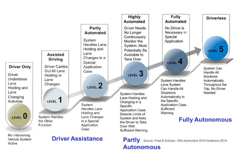
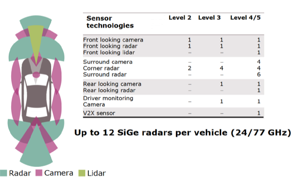
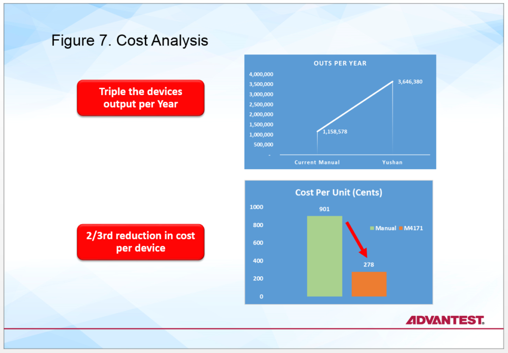
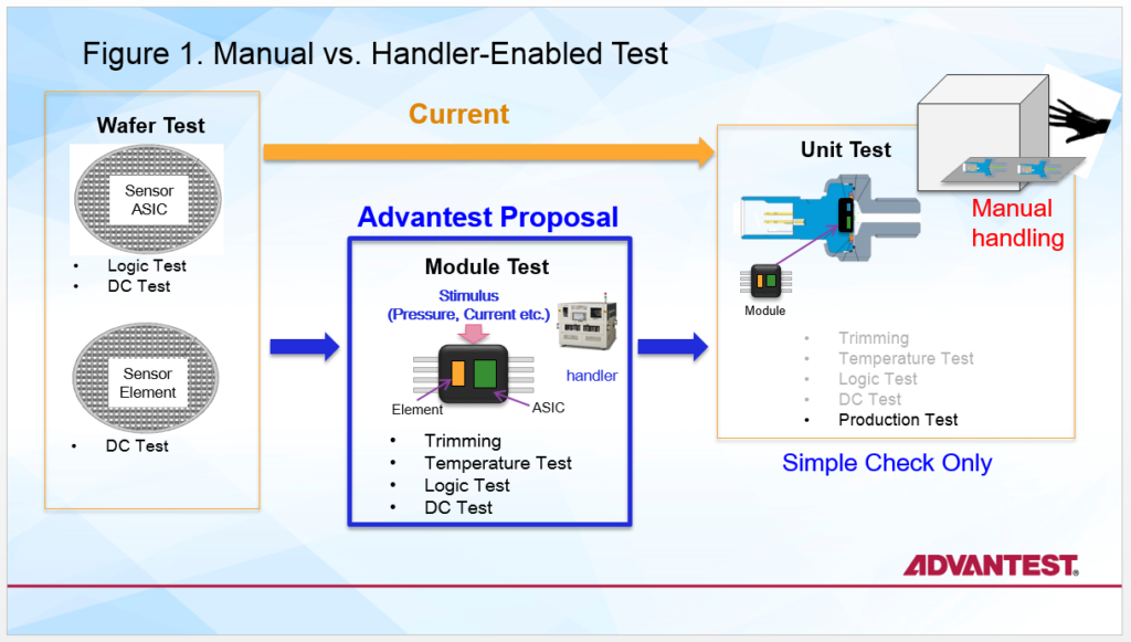
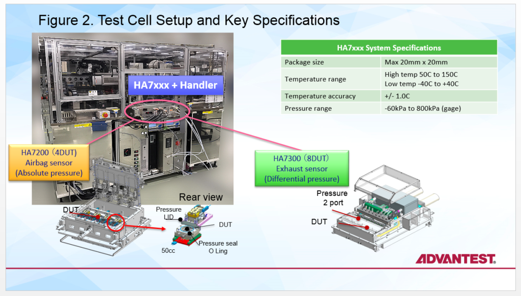
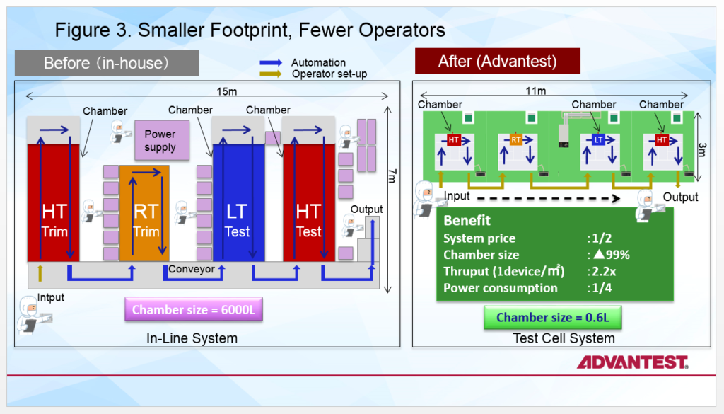
Figure 3. The highlighted lines of code indicate that the SSD never got ready.

In Figure 3, the transaction layer packets (TLP) capture screens indicate that the device kept repolling and returning a value of 0 until hitting the 120-second mark. This means the device did not get ready (CSTS.RDY) and experienced a power-up failure. Once the failure is correctly identified, the information is relayed to the SSD manufacturer, whose challenge is to determine why the failure occurred.

When selected as an option, Advantest’s traffic capture tool runs continually in the background on the MPT3000 platform – essentially as an in-line process, capturing data that may be needed to rerun a test or reproduce an issue. Using the traffic capture tool on the tester allows the user to:

  • Run tests on all slots at the same time and capture the information required to debug issues;
  • Capture the traffic log at the time of the failure without having to reproduce the issue; and
  • Change the amount of logic in the design to capture more information if required. Because the test system is FPGA-based, it is easy to adjust the amount of logic for data capture.

The bottom-line benefit is earlier identification and resolution of device issues, resulting in the faster TTM that device makers require to keep pace with continuing market growth.


Read More