Pages Menu
Categories Menu

Posted in Q&A

Q&A Interview

Doug Lefever, Director, President and CEO of Advantest America, and Managing Executive Officer, Board of Directors, Advantest Corporation

By GO SEMI & Beyond staff

This article was adapted from an interview that originally appeared in the Silicon Catalyst newsletter.

Q: Where does Advantest fit into the semiconductor ecosystem?

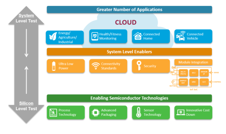
A: As the semiconductor industry has evolved and grown, so has Advantest. We are active throughout the ecosystem, as the figure shows, providing solutions from silicon-level testing up to system-level testing – an area we see having a great deal of potential for growth. Today, our industry-wide involvement reaches beyond our core capabilities in test and measurement to encompass lithography, data logging, consulting and other areas. Oftentimes, folks at startups have done engineering development, but have not been involved in broader business operations, so Advantest can help to bring them along the learning curve. This allows us to form alliances with early-stage companies, which typically don’t need a deep dive into test technology or to get a device onto a tester.

Q: Why does Advantest partner with an incubator like Silicon Catalyst?

A: Because Silicon Catalyst is focused solely on semiconductor solution startups, it provides very early-stage companies with access to goods, services and experience from its network of in-kind partners – all of which are businesses that have been through the startup process. At Advantest, we’re excited to be able to support new startups through our involvement with the incubator. Our commitment comprises 160 hours per month technical education, management guidance, sharing insights and mentoring – the equivalent of one month’s work by a full-time, experienced industry member.

I want to stress that, as these are very, very early-stage ventures, none has yet implemented our actual test resources on its nascent IC designs. We are mentoring and advising them on developing test strategies and manufacturing flows – and, on a broader scale, we are sharing our hard-won experience in running a company. Our business proficiency allows us to perceive where young ventures have weaknesses and help them to address those weaknesses.

These young companies have promising technologies or application ideas, but generally need to gain “ground floor,” startup-level experience. Silicon Catalyst provides opportunities for them to begin building out their teams and to make real connections with equipment and technology providers or financial people, depending upon their stage of development. A key reason that we decided to join the ecosystem is so that we can help figure out ways to reduce the cost of developing and financing new semiconductor startups; funding new technology or anything semiconductor-related has proven challenging to the industry.

We recognize that we’re not going to be selling test systems right away. But a few years down the road, as some portfolio companies that have had access to our technology and our support services become successful, they may gravitate toward our platforms. Advantest does not fund any of these companies or sit on their boards, but we are the only ATE company that gets to help evaluate new companies and new technologies when they ask to join Silicon Catalyst. We can also talk to companies with technologies or IP of interest to us, regardless of whether or not they are added to the portfolio.

Gaining exposure to what’s coming gives us insight into where our industry is headed, what type of equipment customers will need and, perhaps, even the types of performance we might expect from future electronic products. We are gleaning information about emerging technology trends, as well, in such areas as optical, materials, power management, memory cells, MRAM, and low-power memory technology – to name a few.

Q: Where are you seeing momentum in semiconductor startups?

A: As I mentioned, optical is a key trend – many optical-related companies are leading the next wave of high-bandwidth connectivity and low-power computing. While some are building a single chip and others are developing whole modules, the volume of optical products is starting to grow, and high-volume manufacturing (HVM) will be the next step.

In terms of applications, consumer optical-based communications are on the rise. In this area, a new standard is emerging called NGPON-2, which is next-generation Ethernet over passive optical connections. Another area of focus of a number of startups is high-bandwidth computing, while massively parallel computing is enabling advances in artificial intelligence (AI), machine learning and Big Data with shared databases. Dedicated chips are being built for machine learning.

Wearable technology for medical and health-related applications is increasingly incorporating such capabilities as blood monitoring and analysis. One company is making a device that will be able to perform a diagnostic screening on a blood sample at point-of-care without requiring an extensive blood panel analysis. The AI system will be taught patterns consistent with specific pathogens, bacteria or other components so that, when the blood sample is put into the device, the system can determine, within 10 minutes, what’s in there – a much faster and cheaper solution than what’s available today.

Other interesting areas addressing power requirements include low-power memory and energy harvesting, which is wearable technology that uses the heat of your body to charge a battery. The bigger the temperature difference between your body and ambient air, the more energy it puts out.

These are just a few of the technology areas where we are seeing burgeoning opportunities for startups, as well as the industry at large, in the semiconductor arena.

Read More

Posted in Q&A, Uncategorized

Q&A: A Change at the Top

By GO SEMI & Beyond Staff

Yoshiaki Yoshida became Advantest President and CEO in January 2017, replacing Shinichiro Kuroe, who decided to step down after serving in the role since August 2014. Under Mr. Kuroe’s leadership, Advantest returned to profitability in fiscal 2014 and continued to build on that success over the next two years. Mr. Yoshida was elected his successor, and shares here his vision for taking the company forward.

What are your plans for Advantest in your new role?

My goal is to maintain the profitable corporate structure Mr. Kuroe built, while continuing our pattern of growth. I also aim to build a working atmosphere that will further enable Advantest employees to enjoy and take pride in their work.

Are there key topics on which you will focus?

Yes, I plan to focus on three key areas.

First: Our unique value proposition. Everyone values safety and security – both of which our core measurement technologies offer. We have worked hard to ensure that our businesses provide enormous value to people around the world, and it’s essential that we continue to work with confidence to grow our reach.

Second: Our business environment.  Semiconductors are penetrating further and further into everyday life, and semiconductor devices and the equipment and systems that use them will only become more prevalent going forward. With the coming of the Internet of Things, there is no question that semiconductor production and data volumes will grow significantly. This means that test and measurement technologies will play an ever more important role. 

There is still significant room for growth in the application areas for our technologies, from chip test to module and system test, giving us an opportunity to expand our served markets beyond the semiconductor industry, to any and all industries that utilize semiconductors. We must focus on meeting the challenge of applying our core technologies to new and diverse sectors. 

Third: Our position and strengths. Advantest has a strong base of amazing customers, built through our unrelenting focus on providing high-quality products and services. At the same time – and without lessening our focus on satisfying our existing customers – we will shape and evolve our business to embrace new technologies and attract new customers. Another key strength is our financial foundation, built up by our predecessors, which enables us to execute new strategies. But our greatest strength is our employees around the world: our global network and the teamwork of our employees worldwide that support Advantest’s business growth. My mission is to effectively leverage these strengths – customer base, financial foundation and global network – to grow our business and improve corporate and shareholder value. 

To you – our customers, partners and friends – I extend best wishes for a prosperous year. We look forward to playing a role in helping you achieve new levels of success.

Read More

Posted in Q&A

Spotlight on W2BI: Out of the Lab and into the Field: Making IoT Device Testing Portable

Interview with Artun Kutchuk

W2BI, Inc., an Advantest Group company, is a leading developer of wireless device test automation products designed to improve quality and time-to-market for customers’ advanced mobile devices. GO SEMI & BEYOND sat down with W2BI Vice President of Business Development and Strategy, Artun Kutchuk, to talk about the wireless market’s testing needs, why testing Internet of Things (IoT) devices is a different animal with unique testing requirements, and W2BI’s pioneering new approach to testing in the age of IoT.

Q. What are the testing needs for the wireless market in the next five years?

A. The market will undergo rapid change over the next 24 months, let alone the next five years. We will see a move toward connected and aware test environments leveraging both software-as-a-service (SaaS) and platform-as-a-service (PaaS) models. The pace of testing, communication, and information sharing will speed significantly as the types of information that can be shared between R&D and production line systems increase. Future systems will benefit greatly by sharing information with each other – at the chip level, during design and R&D, certification, and returns.

IoT devices have very important test needs: IoT communication modules that power temperature sensors, agricultural sensors, video systems, control systems, biometrics, and the like. As these are deployed in higher volume and defects appear once they’re embedded, it becomes very difficult and costly to pull them out of their environment. The ability to trace pass/fail from silicon all the way to field deployment will require information sharing across test systems, and we’ll start to see further connection both within and between systems to simplify sharing different types of data.

The industry is now in a great position to leverage major advances in the cloud and bring previously disconnected test environments into the connected world. To achieve this, we needed to establish a new product category of connected portable test systems that will replace disconnected test systems for IoT test.

Q. Why do W2BI’s history and skill set position it well to provide test and measurement solutions for the IoT space?

We have a long history in mobile test – handsets, mobile phones, and similar products popular within the last five to ten years in the consumer space. While all of these are now mature industries, our expertise gives us a platform for moving forward in IoT. We perform both feature- and functional-based test, and we have strong expertise all the way through final assembled test. This allows controlling the device under test (DUT) and putting it under many different test scenarios – using an automated approach – to enable fast, thorough testing. Our customer base also positions us well in the IoT market. We provide solutions to top mobile operators, who approve new devices to go on the network. We also build and deliver systems to OEMs, a number of whom utilize them well for a range of applications.

Q. What is your MicroLTE solution, and why is it uniquely suited to address the IoT test market?

A. In the mobile world, an IoT device is purpose-built for specific functions and could have many different communication bearers.  It’s a very different type of device from a tablet or a smartphone – in cost structure, in usability, and in what you have to test on it. The industry needs a test system that can exercise the needs and requirements of an IoT device as well as the development and test cycles that support commercialization.  Our portable MicroLTE solution achieves several things:

  1. Lowers the cost of test. With large-scale economics, you could have one traditional handset provider buy a test system, and then use it to manufacture millions of smartphones. The IoT market has many more manufacturers and is typically much more purpose-built in final use scenarios. These devices are coming to market in large overall volumes, but smaller model volumes and a different cost structure – requiring a different, more flexible approach.
  2. Allows for a different business model. While traditional test equipment typically employs a capital expenditure (CapEx) model, MicroLTE also allows for an operating expenses (OpEx) model. In the IoT space, your testing needs can change rapidly, so instead of acquiring the system on a CapEx basis, you acquire it through a SaaS/PaaS-type subscription, use it for as long as your program needs, and then provide it back to us. We have built a SaaS/PaaS-based cloud system to allow for this approach.
  3. Delivers test portability. The bench test equipment used in mobile feature and functional test is typically big and heavy, and once it’s installed, you really can’t move it with ease. With MicroLTE, we’ve shrunk the test equipment down to fit into the size of a backpack. This makes it easy to transport between sites and use in unique ways and environments. To create this small footprint, we’ve pulled as much functionality as we can off the equipment and put onto a Microsoft Surface Pro 4 laptop with a touchscreen – it’s very small and simple to use and allows the MicroLTE system to provide a rich and functionally complete LTE system, with eNB, IMS, and EPC. 1 Together, these create a rich, portable LTE test lab that’s very easy to learn and use in any environment.
  4. Managed via the cloud. As soon as the MicroLTE equipment comes online, you can manage it remotely via the MicroLTE Cloud Hub built with security and scale via Microsoft Azure. Traditional test systems today are physically disconnected and only physically secured within the facility. With MicroLTE, you can engage the test system with a strong balance of usability, access, and security. The test user can share data in a controlled and managed way to supporting organizations or enterprises, speeding up the R&D and test cycle to allow for a faster time to market.

This system is uniquely suited to IoT because in the IoT world many of the devices have limited human interfaces, e.g., power meters, temperature controls, irrigation controls, parking meters, etc. Thus, automating the DUT is critical, allowing for as little user interaction as possible with the test environment  – consequently optimizing test automation and speeding the test process. We have an extensive background in device automation and take this to the next level with MicroLTE.

Q. What is W2BI’s cloud vision for the future of IoT and assembled device testing?

A. We wanted to solve a couple of problems. First, as we all know, IoT is fragmented, with billions of devices projected by 2020. We needed to build a system that could provide as much test coverage as possible throughout the product’s lifecycle. Second, we wanted to provide a platform for detailed test data to be communicated to different R&D environments, allowing teams to share information easily and quickly for debug, pass/fail, etc. The cloud is the key to providing new and updated test coverage to many systems in a scalable manner, and for bringing together test data from many geographically separated systems. It allows systems to be securely deployed locally or distributed in multiple global regions. Test data is very sensitive, and a cloud-based system lets the enterprise own its own data and manage security consistent with their policies. One customer we are working with has said this cloud design is by far the most secure test system they have seen.

Q. What type of partners is W2BI seeking to extend MicroLTE to the next version?

A. Our first goal was to partner closely with mobile operators, chip/module makers and OEMs. We selected a group of key chip/module makers for the first round of product trials, and it has gone very well. We have just moved from the first phase of development and commercialization to general availability.

For the next phase, we want to focus on the scale of the system for broad deployment and management, so we’re looking at test partners, test labs, companies in the traditional IT space. This will be determined over the next quarter.

We’re enormously excited about this product – it will serve as a complement to Advantest’s production line ATE products while establishing a unique new model for IoT test.

 [1]

eNB = Evolved NodeB base station for LTE radio

IMS = IP Multimedia Subsystem

EPC = Evolved Packet Core LTE architecture

Read More