Pages Menu
Categories Menu

Posted in Q&A

Q&A Interview: Moving Test to the Fast Lane

By: GO SEMI & BEYOND Staff

In this issue, our Q&A interview subject is Steve Pateras, Senior Director of Test Marketing for Synopsys. Steve provides a look at a new test capability, jointly developed by Synopsys and Advantest, that leverages high-speed communication interfaces such as USB and PCIexpress to improve test throughput. (NOTE: This piece was originally intended to serve as a preview of Steve’s VOICE 2020 keynote address; although canceled this year, the conference will return in 2021, as will Steve.)

Q: What was the catalyst for developing this approach?

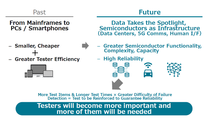
A: The industry is always looking for new ways to improve test throughput, in order to reduce test times and costs. As chip designs get larger and larger, you need more test data, so to keep test costs in line, you need to improve bandwidth to get better throughput.

Moore’s Law kept things growing and increasing in complexity over the past several decades, but periodically, fundamental paradigm shifts needed to happen. The first was in the 1980s, when we moved to structural test because chips had become too complex to cover all possible failure modes using functional verification. Looking only at the I/Os related to flip-flop scan chains, rather than every functional I/O, became the new norm, and this worked well for a couple of decades.

By 2000, scan alone had become inefficient – the number of scan chains and I/Os to scan kept growing larger and larger, and the sheer volume of data was too massive to store on the tester. This led to the next paradigm shift: compression channel I/O. Data is compressed on the tester, then sent to the chip, where it is decompressed on-the-fly into multiple scan chains. Again, this reduced the number of I/Os and test times to a manageable amount. Another 20 years passed, which brings us to today.

As chip features shrink down to 14nm, then to 7nm and beyond, we’re still seeing exponential growth in the numbers of patterns and pattern test data. We’ve again reached the point where we can’t accommodate the volume – even compressed, there is too much data to be stored, and it takes too long to scan data in and out. It’s time for a new approach.

Q: You’re talking about the next paradigm shift?

A: Exactly. Structural (scan) patterns form the primary test for digital logic – more patterns are required to maintain quality, with larger designs requiring more manufacturing tests, and new process nodes demanding advanced fault tests. At some point, things start to break; how do you achieve the necessary bandwidth when you have limited tester speeds and a limited number of available pins? Figure 1 shows real-time bandwidth limitations – that is, the actual number of gigabits you’d need to test some of the newer, larger devices. Existing approaches can’t accommodate moving from tens to hundreds of gigabits per second, let alone into the terabit range. 

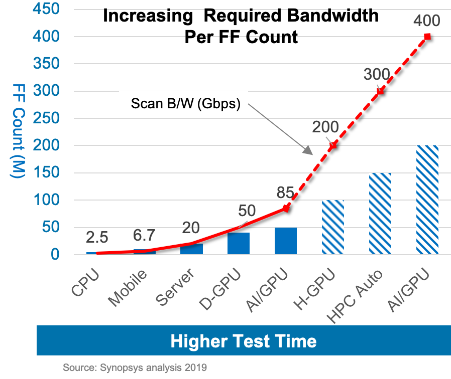
Figure 1. As data volumes increase with device complexity, test times rise sharply.

What we’ve been developing with Advantest is the use of high-speed functional I/O (HSIO) to increase bandwidth. Instead of feeding the compression logic onto the chip via dedicated scan I/O, we’re using very high-speed serial functional interfaces, i.e., USB and PCIexpress, to achieve this. Once the data is entered, we can convert it into the parallel data we need to feed the compression logic. We use these very high-speed serial inputs to get the required bandwidth, and then we parallelize this widely to all the many parallel scan chains on the chip. 

Q: How is the parallelism achieved?

A: Via the on-chip logic that we provide, which works essentially like a transformer. It allows for very large amounts of data coming without the need for dedicated, lower-speed I/Os. We’re essentially reusing the high-speed interfaces that exist on virtually every chip today. Instead of reinventing the wheel and adding more dedicated pins per test, we simply piggyback on top of these interfaces during the test process to send high-speed test data through them [Figure 2].

Reusing these existing high-bandwidth functional interfaces offers three key benefits: it reduces test time; it eliminates the need for dedicated test I/O; and it provides test portability through the product lifecycle. 

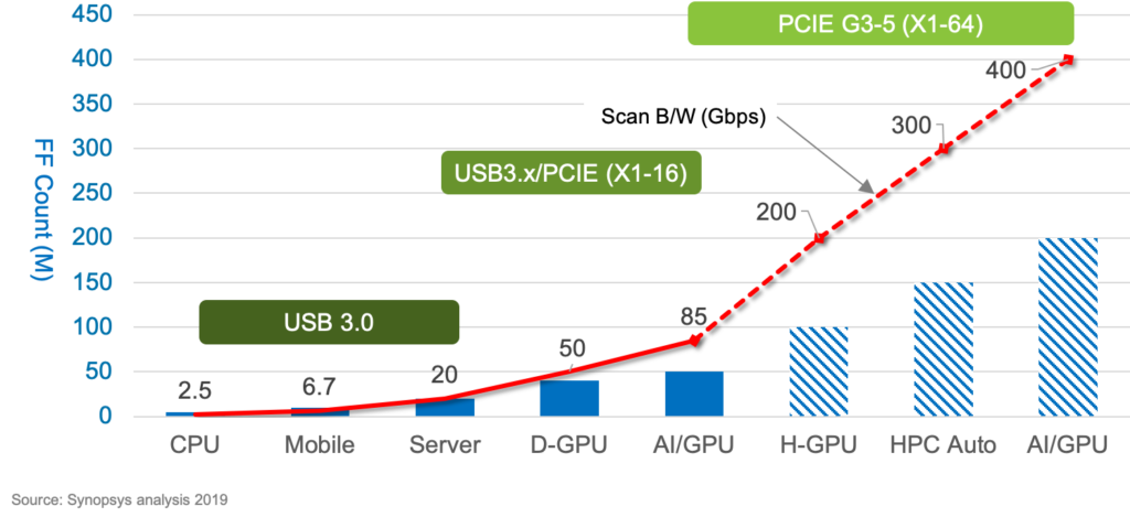
Figure 2. Reusing HSIO protocols improves scan bandwidth, significantly lowering test times.

Q: How long has the new solution been in development, and what does it entail?

A: We’ve been working with Advantest on this new HSIO paradigm for over two years, combining key components from our TestMAX suite of software with Advantest’s V93000 SoC tester. The solution entails three key aspects, summarized in Figure 3:

  1. Packetizing manufacturing test data to accommodate HSIO protocols. Integrated into the V93000, our software [dark green box] takes traditional parallel data from ATPG tools, converts it into high-speed packet data, then depacketizes the data coming back and maps it to known failure descriptions.
  2. Enabling the tester to accommodate this approach [light green box]. Testers themselves need to be able to drive data through these high-speed interfaces, so through this joint effort, Advantest has added new hardware onto the V93000 to provide the HSIO function and ensure their SmarTest software can work with it.
  3. Ensuring the chips can handle this high-speed packet data. We devised a bidirectional HSIO-to-DFT interface controller, which is added to the chip as IP [dark grey box] to actively manage incoming high-speed packet data on one end and receive the parallelized lower-speed test data on the other.

HSIO Test Paradigm Diagram

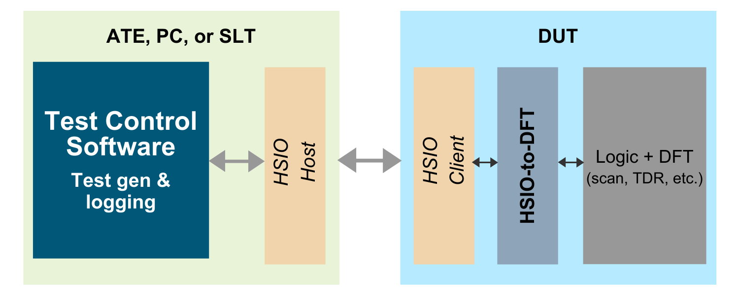
Figure 3. The new HSIO test paradigm integrates key software, hardware and on-chip functionality.

In addition, our Adaptive Learning Engine (ALE) adds more intelligence to the test process. It allows our software to actively look at failure data coming back from the device and adapt the test to deal with the kind of failures that are being seen on the tester, as well as perform more advanced diagnostics. This can be performed locally on individual testers, as well as on a Big Data level – each tester on the floor can send its results to a centralized analytics engine analyzing results and looking for systematic issues across multiple devices over time. In this way, we can help to greatly improve the test process at the test-floor level.

For more details, real-world examples and updates on this new high-speed functional I/O test paradigm, make plans now to attend Steve’s keynote address at VOICE 2021 in Scottsdale, Ariz.

Read More

Posted in Q&A

Q&A Interview – Judy Davies, Advantest


By GO SEMI & Beyond staff

As COVID-19 continues its global spread, tech conferences and tradeshows are being postponed or outright cancelled to help protect the health of attendees, exhibitors and organizers. Advantest joined this effort with its VOICE 2020 Developer Conference, cancelling the Shanghai event and rescheduling the U.S. event in Scottsdale, Arizona, to September 29-30. Judy Davies, VOICE Ambassador and vice president of Global Marketing Communications, Advantest America, shares the company’s perspective on the outbreak and its impact, and offers a hopeful note for our industry and our world post-pandemic.

Q. What made you decide to reschedule the U.S. event as a live conference later in the year instead of holding a virtual event?

A. We actually did put on a virtual event, but this did not extend to VOICE 2020, which we really want to keep on the calendar. When large events such as the Mobile World Congress and the SEMICON China and Korea shows were cancelled, we needed a way to get technical information out to our customers and users – especially those in Asia, the first region impacted by COVID-19. To that end, we held our first virtual tradeshow in early March. We had nearly 200 attendees from 47 countries, with sessions presented in multiple languages by a global group of speakers. It’s such a great example of everyone pulling together to demonstrate their commitment to the industry and their empathy for the situation that we’re all facing. Instead of backing out – which would have been understandable – all the presenters were eager to participate.

This attitude has carried over to our program for VOICE U.S. Instead of cancelling, we have opted to postpone VOICE 2020 because Advantest is a leader in sharing technical information and this event is so important to our customers. By choosing a date later in the year, we’re looking to strike a balance – doing what’s necessary now, while continuing to innovate and maintain our industry-leadership role. We hope and believe that, by September, holding VOICE U.S. in person will be feasible. Everyone involved with the event has been accommodating and encouraging, stepping up to reaffirm their participation. Each of our four keynote speakers is confirmed for the new dates, as are our sponsors and exhibitors.


Q. Optimism and team spirit is certainly important right now. How does the theme of VOICE 2020 reflect this attitude?

A. The theme of the conference this year is “Your Voice. Your Vision. Our Value.” Advantest is here to support our customers – we hear their voice, we see their vision, and we partner with them to make it a reality. It really embodies our own vision (Adding Customer Value in an Evolving Semiconductor Value Chain) and our “INTEGRITY” core values. We don’t just give lip service to this concept – integrity is central to everything we do. We put together VOICE with this in mind, developing a program that truly reflects what our customers want and need to know to help them do their jobs even better.


Q. Speaking of the program, who will be delivering the keynote addresses this year?

A. We have a stellar lineup that comprises experts from within and outside the industry. On September 29, we’ll feature two keynotes on the future of test and technology. First, Steve Pateras, director of marketing for the Test Automation Group at Synopsys, will deliver a speech titled “Test Evolves – New Access to Adaptive Learning.” Following Steve will be Dr. Kate Darling, research specialist with MIT Media Labs. An expert in robotic ethics, Dr. Darling will discuss the future of human-robot interactions. On September 30, Dan Hutcheson, the well-known CEO of VLSIresearch Inc., will address 5G, IoT, AI and other critical IC markets, as well as some of the key industry trends he has identified and is following. Last, but not least, Fredi Lajvardi, vice president of STEM Initiatives at the Si Se Puede Foundation, will share his fascinating story about how he turned a group of high school students into a national-champion robotics team, beating top-ranked teams at the university level. I’m really excited to see all of these speakers.


Q. What else will VOICE 2020 hold in store for attendees?

A. The technical program has become known for the richness of the content provided. Our focus this year is on 5G with the theme being “5G: Made Real by Our Customers, Made Possible by Advantest.” Again, the focus is always on the customer and on the role we can play in helping them bring their ideas and plans to fruition. The program will feature nearly 70 papers divided into seven tracks, including new tracks on 5G/millimeter wave, parametric test and hot topics such as AI and machine learning. We’ll also feature our Partners Expo and several networking opportunities, including the off-site welcome reception and technology showcase on Monday night, September 28. And immediately following VOICE, we will conduct the Workshop Day on October 1.


Q. What else would you like readers to know?

A. I just want to reiterate how grateful I am to everyone involved with VOICE. This includes not only our keynote speakers, sponsors and other participants, but also our marketing team and the VOICE steering committee for all the hard work they’ve put in to make these events happen. Especially when there’s so much uncertainty right now, I can’t imagine being part of a company that is any more focused on partnering with and showing compassion for its customers.

I read recently a couple of quotes that summarize the notion that we’re all in the same boat, so to speak. Xiaomi, a Chinese consumer electronics company, donated thousands of face masks to Italy’s government, and on the crates was printed a quote from the Roman philosopher Seneca: “We are waves of the same sea, leaves of the same tree, flowers of the same garden.” Similarly, boxes of masks sent to China from Japan bore a quote from a Tang dynasty poem reading, “Foreign lands separated by mountains and rivers, we share the wind and moon under the same sky.”

Now, more than ever, these quotes truly resonate for Advantest. We have 5,000 employees, more than 80% of whom are located outside of the U.S., but we are all part of one world, and we are resilient. Things may be challenging right now, but we’ll get through it, together.


Read More

Posted in Q&A

Q&A Interview with Scott West – Expanding SSD Test Capabilities for Extreme Temperatures

Advantest has found great success with its test solutions aimed at the solid-state drive (SSD) market. In this issue of GO SEMI & Beyond, Scott West, Product Marketing Manager for System-Level Test, provides some background on how the company began to address this market, and shares details on its latest SSD offering, the MPT3000ARC, for validation testing to accommodate extreme thermal standards. 

Q: What was the catalyst for developing this latest addition to the MPT3000 family?

A: Let me briefly recap the MPT3000’s evolution. After spending several years on product research and development, we launched the SSD platform in 2014, signaling a branching out for Advantest from chip test to system-level test. While chips are a single unit, manufactured all at once, with everything controlled by the chipmaker, SSD drives are themselves systems. They’re modules that contain a great deal of flash memory, a controller, controller circuitry, protection capacitors, and other components, which adds further complexities from a test standpoint.

Our focus from the start has been to test SSDs through a protocol interface, including the three primary SSD protocols: SATA [Serial ATA], SAS [Serial Attached SCSI] and PCIe [PCI Express]. All products in the platform test all of these protocols, including PCIe Gen 4, the latest version of PCIe, which is about twice the speed of Gen 3. However, with the ARC system (see Figure 1), we’re expanding in a different direction – we’re looking not just at all SSD protocols, but at all test insertions.

Q: How does this differ from the other MPT3000 products?

A: Each product in the platform has a slightly different, and specific, purpose. The MPT3000EV2 (the second generation of the 3000ENV) is a large-chamber system for reliability demonstration testing (RDT), which is focused on the test design. This involves constant hot and cold temperature cycling of several hundred drives over many months. For example, there is one project we are working on that requires more than six months of constant temperature cycling and testing.

The MPT3000HVM is a rack system designed for production test. It tests each individual drive during high-volume manufacturing to make sure it’s good. It requires not months but several hours, under hot conditions only, with a large amount of power pushed through, to validate that each drive works as expected. It can test quickly because of the rack design – you can put in one drive and immediately begin testing while you’re loading more.

The ARC system addresses a couple of key parameters that the other systems in the family don’t with respect test insertions. The first is extreme temperature range. The standard is referred to as automotive range (-40°C to +105°C), which is where the product name is derived from – ARC stands for Automotive Range Chamber. But automotive is only one application; the standard is also used in aerospace, defense and other ruggedized applications that require extreme temperature range.

The second parameter is high-volume production cold-temperature test. The new chamber was designed to be able to accommodate this type of testing in the production environment, for which the EV2 is not as well suited as it is optimized for very test times. In the enterprise, cold temperature – down to as low as -40°C – is often required for production test. The MPT3000ARC can test up to 128 PCIe Gen 4 DUTs in parallel. Because you have to load the entire chamber at once at ambient temperature, it doesn’t make sense to make it too big, as the ergonomic range needs to be production friendly.

Q: Do all the MPT3000 products have the same pin electronics?

A: Yes, all the systems are compatible with respect to the software and firmware, and all electronics that go to the DUT come from the same test electronics boards. The systems feature up to 22.5G electronics with tester-per-DUT architecture.

However, the ARC system interface boards, which are designed for the system’s thermal interface, are different from those for the HVM. In the ARC chamber, the chamber is turned on its side, with up to four primitives inserted vertically instead of horizontally (see Figures 2 and 3). This creates a totally closed system that allows air to circulate from right to left inside the chamber, whereas the HVM rack-based system pulls air from the room and then blows it to the back of the system and out into the room. The ARC chamber also features a pocket door designed to accommodate the ergonomic requirements of manual loading and to be automation friendly as well

Q: What are some other key features of the MPT3000ARC?

A: As I mentioned earlier, the system has the ability to test up to 128 DUTs of 50W each. The primary compressor stage has a water-cooled condenser that transfers the energy generated by the chamber load to the test floor’s water-cooling system. This construction helps regulate chamber temperature to ensure consistency. The system has two programmable power supplies for PCIe DUT, targeting high-power enterprise SSDs, and performs current and voltage measurement with high accuracy.

We introduced the MPT3000ARC at the Flash Memory Summit in August 2019, where it was very well received, and the system has shipped to the first customer. We look forward to sharing further successes and advancements in the future.

FIGURES

Figure 1. The MPT2000ARC is the latest addition to the MPT3000 family of SSD testers, and tests devices to extreme temperatures.

Figure 2. The chamber for the MPT3000ARC is oriented vertically to allow a fully closed system with right-to-left air flow. The primitives are stacked 2×2, back to front. 

Figure 3. This view inside the ARC chamber shows the positioning of one of the lower primitives in a 64-DUT system.


Did you enjoy this article? Subscribe to GOSEMI AND BEYOND

Read More

Posted in Q&A

Q&A Interview with Dieter Ohnesorge – 5G mmWave Challenges and Solutions

By GO SEMI & Beyond staff

mmWave is the key topic when it comes to frequency ranges that allow to allocate more bandwidth. millimeter-wave (mmWave) is the band of spectrum between 24 GHz and 100 GHz. As it enables allocation of more bandwidth for high-speed wireless communications, mmWave is increasingly viewed as one key to making 5G connectivity a reality. In this issue, Dieter Ohnesorge, product manager, RF solutions for Advantest, discusses the market opportunity and test challenges associated with 5G mmWave, as well as Advantest’s solution for addressing them.

Q. We’ve been hearing about the promise of 5G for a long time. What demand drivers are edging it closer to fruition?

A. If you look at the global ecosystem [Figure 1], there is massive potential for 5G in many vertical markets. For example, 5G will be an essential aspect of smart manufacturing (SM). SM processes provide greater access to real-time data across entire supply chains, allowing manufacturers and suppliers to manage both physical and human resources more efficiently. This will result in less waste and system downtime and will make more technology-based manufacturing jobs available.

Remote access to health services is another key benefit of 5G. First, it would mean less driving, which is much better for the environment as well patients and doctors and staff. Second, if you’ve already had a screening and the doctor has access to it, why not communicate remotely, saving time on both sides? With 5G, you have the benefit of high bandwidth and low latency, which is important for many applications. Autonomous driving, consumer multimedia applications, and remote banking are just a few more of the many areas that will benefit from highly reliable connections, as well as high bandwidth and/or low latency.

Figure 1. A global ecosystem of vertical deployments stand ready to benefit from 5G.

Q. What has prevented 5G from becoming fully implemented?

A. Primarily, the infrastructure requirements. A specification of this scale cannot be implemented on a local basis alone – it takes a concerted, global effort. The worldwide effort to achieve 5G standardization is a huge step forward. In the U.S., discussions about mmWave technology are currently under way, and at the end of the year or early next year, the discussion will expand towards 5G in the <6GHz band.

In 2015, Verizon took it upon themselves to define a proprietary version of 5G as the next step forward from the current 4G LTE standard. At the end of 2018, the 5G NR (New Radio) industry standard developed from the Verizon effort was released, and all new deployments will follow this spec. In the U.S., initially the frequency band is 28 GHz, with carrier bandwidth of two 425-MHz channels and 24 GHz with seven 100 MHz channels. Additional frequency bands will be auctioned by the FCC for 37, 39 and 47 GHz from December 2019 onward. Other mmWave activities can be seen all over the world, although at different pace.

Q. Where does mmWave come into play?

A. Because the portion of the spectrum that mmWave covers is largely unused, mmWave technology can greatly increase the amount of bandwidth available, making it easier to implement 5G networks. Lower frequencies are currently taken up with the current 4G LTE networks, which typically occupy between 800 and 3,000 MHz. Another advantage is that mmWave can transfer data faster due to the wider bandwidth per channel, although over a shorter transfer distance – up to around 250 meters, or just over 800 feet. This means that it could conceivably work as a replacement for fiber or copper wire into homes and businesses, and this “last mile” capability would broaden the reach of 5G to cover both small and very large areas.

Q. What are the challenges around mmWave test that spurred Advantest to develop a solution? Which does it address?

A. Advantest’s Wave Scale RF card for the V93000 tester platform has seen great success. Its operational range is 10 Mhz to 6 GHz, so we needed a solution that can address the frequency and power requirements associated with higher-bandwidth devices.

Frequency is one of the key parameters associated with mmWave, and with that comes power-level measurement, EVM [error vector magnitude], ACLR [adjacent-channel leakage ratio], and other aspects that all need to be addressed in the testing process to ensure they meet specifications at the wider bandwidths required by 5G-NR.

Another requirement is the number of ports – with 5G mmWave’s beamforming capability, testing could easily be in the range of as many as 32 to 64 ports. At the same time, due to the frequency nature of mmWave, with 5x to 7x frequency, the cost goes up as well. That’s also been one of the challenges: holding down the cost of test with a wide number of sites being tested in parallel.

The V93000 Wave Scale Millimeter test solution, which we introduced in May 2019, extends the capabilities of Wave Scale RF. It is designed for multi-band mmWave frequencies, offering high multi-site parallelism and versatility. It has two operational ranges: 24 GHz to 44 GHz for 5G mmWave, and 57 GHz to 70 GHz, which extends the product’s capabilities for the wireless Gigabit, or WiGig, era. Figure 2 shows the range of frequencies that Wave Scale was developed to cover.

Figure 2. Wave Scale RF provides a scalable platform for connectivity device test, from standard RF to millimeter-wave.

In addition, new modules can be added as new frequency bands are rolled out worldwide. The card cage has up to eight mmWave instruments, making it versatile, cost-effective, and able to perform as well as high-end bench instruments. Because it has wideband testing functionality, Wave Scale can handle full-rate modulation and de-modulation for ultra-wideband (UWB), 5G-NR mmWave up to 1 GHz, and WiGig up to 2 GHz, supporting probes as well as antenna-in-package (AiP) devices connectorized, and over-the-air testing.

Figure 3 illustrates 5G device measurements that can be achieved using Wave Scale Millimeter: power out/flatness test results. The solution’s massive parallelism allows these tests to be performed quickly and at significant cost savings.

Figure 3. This graph overlays a customer’s 8-channel transceiver power-out test results, performed over 800 MHz at 28 GHz. Wave Scale allows channel flatness to be executed in a single operating sequence, one channel after the other.

Q. When will this solution be widely needed?

A. The Industry is still learning how to test these devices. We can help customers get started now, thanks to the modularity of the solution. They can start below 6GHz and when they need the higher frequency, we can add the mmWave capability.

The bottom line is that Advantest’s platform approach is ideal for this scenario – because it is scalable and modular, we can continue to add to the product’s functionality to make it even more comprehensive. By being ahead of curve, we will have the right solution ready when our customers need to adapt to new requirements.


Did you enjoy this article? Subscribe to GOSEMI AND BEYOND

Read More

Posted in Q&A

Q&A Interview with Keith Schaub

By GO SEMI & Beyond staff

The use of artificial intelligence (AI) techniques such as machine learning is growing as the semiconductor industry discovers new ways to use these approaches to do things that humans cannot. In this issue, we talk with Keith Schaub, Vice President of Business Development for Advantest America’s Applied Research Technology and Ventures, about unique research Advantest is conducting with the Univ. of Texas, Dallas, to integrate machine learning into a challenging area of chip development: RF transceiver design, test and manufacturing.

Q. What led Advantest to begin investigating the use of machine learning for this application?

A. Machine learning has been around for a long time. It’s actually a subset of AI, by which machines learn how to complete tasks without being explicitly programmed to do so. There have been many startups over the years that looked to leverage machine learning, but it’s never really been implemented previously within the semiconductor industry. As we have begun to do more work looking at the potential advantages of using AI, we’ve come to realize there are some practical applications by which the industry could greatly benefit.

Q. What is the approach you’re developing for implementing machine learning?

A. The approach we’ve been working on with UT Dallas is a proof of concept for how to take a machine learning method and apply it to semiconductor manufacturing and test – specifically, RF transceivers. Machine learning is much better suited to analog than to digital devices. Digital is a series of 1s and 0s, so the system can either recognize something or not, but there’s no ability to drill down in terms of granularity in order to leverage the more powerful aspects of machine learning. Analog systems require far more data because they’re more complex, making them a better environment for machine learning.

In RF applications, the numerous transmission protocols, large amounts of data, and large bandwidths with high data rates create challenges that call for the development of new algorithms for which modern machine learning is well suited. RF transceivers are affected by a variety of impairments, such as compression, interference and offset errors, as well as IQ imbalance. IQ signals form the basis of complex RF signal modulation and demodulation, both in hardware and in software, as well as in complex signal analysis.

Figure 1 shows a typical RF transceiver circuit, with a number of potential noise errors highlighted in red. A graphical representation of the signal quality can be generated to correspond with each error (Figure 2). The challenge for the operator is knowing which error generated which plot, and which errors are the most problematic.

The approach we’ve developed is a machine learning-based solution for noise classification and decomposition in RF transceivers. The machine learning system can be trained to learn and then identify and match up each impairment to each noise plot; this is something that would be virtually impossible for a human to do.

Figure 1. RF circuit with potential noise errors in red.

Figure 2. Constellation plot showing signal quality impairments caused by various noise errors.

Q. How would this be put to use in a manufacturing environment? 

A.  Figure 3 illustrates how the machine learning solution works. During the training process – this is literally how the system learns to recognize and classify data – a set of constellation points from early versions of the ICs being developed are fed into a machine learning system. Extracted features are separated by category as either noise-type classification or noise-level regression, with the system learning what each type is and how to separate and recognize them by individual error. This is indicated by the different colors assigned to each specific noise type. This is particularly valuable because, while RF transceiver designs, like those of most analog circuits, involve a high degree of customization, certain types of noise errors can potentially occur regardless of the specific circuit.

Once the training process is complete, the system can be put into use in production mode with actual DUTs [devices under test], and use what it has learned through the training process to apply models, identify the various types of errors and provide an impairment report. The system doesn’t have to go through lengthy downtime because the assessment can be completed quickly, and the resulting report allows the user to determine which errors are most critical and need to be addressed so that no damage or yield loss occurs.

Figure 3. Machine learning process for RF transceiver noise classification and decomposition.

This approach can be used throughout the test process – not only for device and system-level test, but also during design-for-test, so that analog/RF designers can better simulate and understand whether their designs will work. This is important due to amount of hand/custom work and the number of variables associated with analog device design.

Q. At what point do you see this technique being broadly adopted in the industry? What challenges would prevent this from occurring?

A. While the technology is mature enough that it could be implemented right away, there are several reasons machine learning has not yet been broadly adopted in the semiconductor industry. For one, there haven’t been sufficient resources/datasets to support its widespread use. For another, the industry is highly risk averse and concerned about security, so companies don’t want to make their data – which is their valuable IP – available for the machine learning process. They have it in the cloud, but in their own individual clouds, which don’t talk to each other. My belief is that use of machine learning will become widespread when the big IDMs [integrated device manufacturers] take the initiative, and the rest of the industry will follow suit.

NOTE:

Advantest’s Applied Research Technology and Ventures group would like to acknowledge the recent publication at the 2019 IEEE 37th VLSI Test Symposium (VTS) of a paper titled “Machine Learning-based Noise Classification and Decomposition in RF Transceivers,” which details the work described in this interview. The paper was jointly developed by Deepika Neethirajan, Constantinos Xanthopoulos, Kiruba Subramani, Yiorgos Makris (UT Dallas), Keith Schaub and Ira Leventhal (Advantest America).

Read More

Posted in Q&A

Q&A with Advantest President & CEO, Yoshiaki Yoshida discusses the mid-term plan, Grand Design

By GO SEMI &  Beyond staff

The subject of this issue’s Q&A is Yoshiaki Yoshida, president and CEO of Advantest Corporation. He joined Advantest in 1999 and held a succession of leadership positions prior to being elected to his current roles in January 2017. He holds a degree in management from Yokohama National University. Mr. Yoshida recently introduced new business strategies that will guide Advantest’s business both in the near term and over the next decade.

Q. What were the trends that helped Advantest achieve the strong financial results for FY2017?

A. Advantest’s FY2017 financial year-over- year growth of 32.9% can be linked to several key industry trends. Strong demand for 3D NAND flash memory and DRAM led memory chipmakers to actively invest in expanding their production capacity. In addition, high-performance computing (HPC), artificial intelligence (AI), display driver ICs, and automotive ICs and sensors amid advancements in automotive electronics – combined with demand for data center-related semiconductors – were major contributors.

Q. Advantest has developed a “Grand Design” plan. What market / industry advances led to the development of this plan?

A. Amidst the digital transformation driven by semiconductor evolution, Advantest’s business environment is changing dramatically. With the explosion of data driving developments in semiconductor technology, the tester market is evolving in concert with the semiconductor space. Whereas chip drivers previously evolved from mainframes to PCs and smartphones, semiconductors are now becoming the infrastructure of a data-centric future, as complex applications including data centers, 5G communications, and human/machine interfaces move into the spotlight. [See Figure 1.] These applications require more complex semiconductors with greater capacity and functionality – and, in turn, test systems that can accommodate their advanced testing requirements.

Figure 1. Changes in the semiconductor market.


To capitalize on these successes and take full advantage of the industry environment, we developed the 10-year Grand Design, as well as the Mid-Term Plan, which covers FY2018 through FY2020.

Q. What are the key aspects of each of these plans?

A. The vision of Advantest’s Grand Design is to add customer value in an evolving semiconductor value chain. More specifically, we will further contribute to the semiconductor industry by enriching, expanding and integrating our test and measurement solutions throughout the entire value chain. [See Figure 2.] Our business is organized into three reportable segments: (1) semiconductor and component test systems; (2) mechatronics; and (3) services, support and other activities to address the wide-ranging needs of customers in every area of the industry ecosystem.

Figure 2. Advantest’s Grand Design involves expanding on its existing business areas to ensure its test technology is adopted and integrated throughout the semiconductor value chain.

Q. Why is Advantest uniquely positioned to successfully implement these business plans?

A. We have a number of advantages working in our favor.

  1. We have the world’s leading product portfolio, built on highly scalable, modular platforms, and we hold a dominant position in several key growth areas, including DRAM, non-volatile memory (NVM), HPC and networks.
  2.  We have the number one global customer base, developed and nurtured over many years, with a very strong presence in fast-growing Asia markets.
  3.  We offer complete test environments, including chip-handling tools and device-interface peripherals, and we have strong, comprehensive support teams in every region we serve. We are excited by the opportunities afforded by the current state of the industry, together with our already strong and well-established position in the global semiconductor ecosystem. We look forward to making great inroads with our near- and long-term plans, and to reporting on key successes and innovations that will enable us to achieve our objectives, strengthen our portfolio, and become the number one provider of test and measurement solutions.

Yoshiaki Yoshida Advantest President & CEO

Read More