By Ulrich Schoettmer, Product Manager, and Frank Hensel, Application Expert, Advantest
Data rates for serial interconnect technology in CMOS are continuing to grow, driving the concurrent need for new instrumentation in automated test equipment (ATE).
Current serial technology has reached maturity – for example, PCI Express (PCIe) 2 and 3 running at 5 and 8 gigabits per second (Gbps), respectively, or SATA II running at 6Gbps – so robust standard library cells are available for various CMOS process nodes. For volume production, most manufacturers rely on DC tests, internal and external loop back tests, and therefore don’t require specialized high-speed ATE instrumentation.

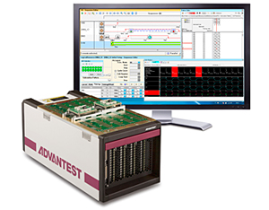
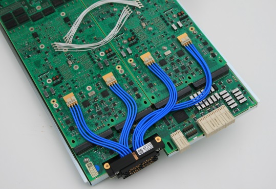
Figure 1. The Pin Scale SL is a fully integrated ATE instrument for super-high-speed operation.
However, the picture changes a bit when it comes to interface technology, which steps up to speeds of 10Gbps and higher. Particularly in the area of network processors, emerging advanced SerDes technology runs at data rates of 10, 12 and 15Gbps. These interfaces are operating in groups of eight or more lanes as “super-speed highways” in chip-to-chip or chip-to-peripheral links. Given the high levels of quality required, at-speed validation in manufacturing test is advisable to ensure that critical signal fidelity parameters are met at nominal data rates.
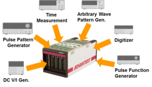
To meet this demand, Advantest developed a super-high-speed card for its V93000 tester platform: the Pin Scale Serial Link (SL). The Pin Scale SL instrument extends the speed and performance capabilities of prior cards in the Pin Scale family.
The Pin Scale SL is designed for SerDes, which is the serial technology used for such industry standards as PCIe, Serial ATA (SATA), Universal Serial Bus (USB) and a variety of networking interfaces. Transition to SerDes I/O links initially required significant design and validation efforts, which have proven worthwhile given SerDes’ overall benefits compared to conventional parallel I/O. These include better bandwidth, fewer I/O pads, and robustness against interference.
With a pin electronic which meets a bandwidth of 16Gbps, Pin Scale SL can serve the engineering and production needs of advanced SerDes technology. The new instrument comes with eight differential drive and receive lanes, each, on a single card.
Unique Properties of Digital High-speed I/O Interfaces
Serialized signals, instead of running off of a parallel bus, are packaged (serialized) onto a narrow path, so the serial path’s raw data rate has to be much faster to carry the same net bandwidth. Higher data rates go along with higher power, unless the signal amplitude is not minimized, but small signals are susceptible to interference and ground bounce. Therefore, serial links are usually implemented as differential lanes, which are far more immune to common mode noise. Due to the increased data rate, transmission line methodology also comes into play, so impedance control and termination become relevant.
At data rates greater than 10Gbps, frequency-dependent losses become a serious factor in printed circuit boards or cabling design. The I/O cells thus contain both active pre-emphasis structures on the drive side (finite impulse response, or FIR-based) and decision feedback equalization (DFE) on the receive (RX) side to overcome signal distortion and recover data. This makes the analog properties more complex and sensitive to process margins than in previous generations of chip design.
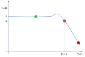
Figure 2. Typical PLL bandwidth characteristics.
To simplify signal distribution, the clock reference transmission is eliminated by embedding the clock into the data stream, which leads to such encoding schemes as 8/10-bit encoding. Such coding guarantees a minimum transition density, which is the prerequisite for the clock data recovery (CDR) circuits on the receiver side to extract the clock signal from the (recovered) data stream and sample the incoming data. To ensure that the CDR circuits synchronize the sampling clock properly, it’s very important that the phase lock loop (PLL) circuit operates with minimum jitter and tracks phase variations of the incoming signal (see Figure 2). On top of the physical encoding, a transaction protocol is often utilized to organize and synchronize the data handling and ensure proper receipt of packets.
The typical list of tests needed to validate proper operation of the SerDes circuitry includes the following:
DC tests
Active equalization on the drive side is accomplished via dynamic variation in drive strength, creating a network of different current source settings that must be validated and may require trimming to work properly. Similarly, on the receive side, impedance matching resistor networks are used, which require trimming. As a result, precision DC tests are required to check output levels, swings and currents across the various settings, as well as precision leakage measurement, impedance measurements and the like.
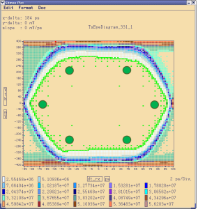
Figure 3. Eye diagram with 6-point mask
Pin Scale SL serves these needs by providing integrated parametric measurement units (PMUs) with accuracies in the <2mV and +/- 10nA range. These PMUs are available in parallel on each I/O pin, which allows full parallel measurements, minimizing test-execution times in production.
Dynamic AC tests
Dynamic AC tests validate the functionality of the SerDes blocks at nominal data rates. A common methodology for the TX side is to perform an eye margin test and a total jitter test. While a high-bandwidth oscilloscope is suited for performing such tests in the bench environment for engineering purposes, a more streamlined multi-point eye mask test can be performed in the ATE environment, as shown in Figure 3. In the ATE environment, the measurement follows a bit error rate (BER) of a pattern stream-based approach, which allows for test coverage on both the TX and RX sides. For this task, the device under test (DUT) is turned into a test mode to generate a pseudo random binary sequence (PRBS) at full data rate, while the ATE receiver is used to scan the data stream along the voltage and timing, or phase, axis.
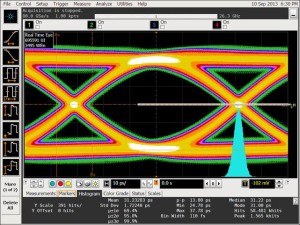
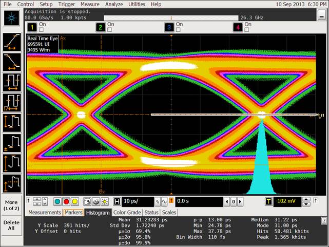
Figure 4. Signal quality of Pin Scale SL at 16Gbps using PRBS 7.
High-resolution verniers (i.e., movable graduated scales) for comparator threshold and sampling timing allow collection of detailed shmoo plots (much like a sampling scope plot) or may be used to scan to “open eye area” for eye width and height against a predefined multi-point mask. For very fast collection of total jitter budget measurement, a time measurement unit available on the Pin Scale SL card per pin/lane comes in very handy.
On the RX side, it becomes important to stress the signal recovery properties of the circuitry. For that matter, the ATE instrument sends PRBS signals to the DUT with high fidelity, an example is shown in Figure 4. By adding additional distortion (highly attenuated signals) and/or with superimposed jitter. Signal properties like drive amplitudes, signal equalization and jitter-injection generators are the programmable tools that come to play in order to emulate real-world, worst-case DUT conditions.
Additional Measurements
Frequency offset tests are relevant to validate that the “remote” end of the communication path properly synchronizes to the data stream, especially in the networking application space. As a result, emulating a certain frequency (phase) offset between the TX and RX data streams to make sure the CDR still syncs properly is a mandatory test process. Programmable frequency verniers, down to the parts per million (ppm) offset versus nominal settings, are very helpful. Test vehicles for these tests are also PRBS signatures. Pin Scale SL supports the above tests via programmable PRBS generator and analyzer hardware blocks, which, again, are available on a per pin/lane basis.
Generic ATE tests
Besides their high-speed specific properties, these pins often also serve as the structural access path for all sorts of logic scan tests. For that purpose, the high-speed instrument also has to support “classic” pre-stored vector generation and truth table compare. Pin Scale SL also supports this use model and features a full-blown digital vector generation and compare engine behind every single node, which is fully compatible with Advantest’s mainstream digital pin card offering (Pin Scale 1600).
Protocol emulation support in HW
Pin Scale SL features a standards-compliant PCIe protocol stack, which allows high-level communication to the DUT. Other protocols, e.g. SATA, are also under development.
Looking Ahead
The Pin Scale SL Instrument provides enough headroom to be ready for the next generation of ASIC designs, which will be running 15Gbps links. PCI Express Gen 4, which is also under development, will be running 16Gbps and is anticipated to start emerging in 2015/2016. Besides standards, a number of proprietary SerDes links are under development that fall into the sweet spot of Pin Scale SL availability.
Read More