Pages Menu
Categories Menu

Posted in Featured Products

Photoacoustic Microscope Furthers Research in Dermatology and Regenerative Science

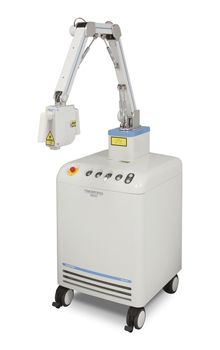
A new photoacoustic microscope introduced by Advantest enables non-invasive imaging of blood vessels in the dermis to a depth of 3mm, affording researchers in regenerative medicine an alternative to conventional biopsies.  Unlike biopsies – which have shortcomings, including limited insight into changes over time – Advantest’s new Hadatomo photoacoustic microscope offers researchers a thoroughly non-invasive process, with an ability to easily reference and compare historical results. This new evaluation method is poised to contribute to further advances in regenerative medicine, dermatology, and plastic surgery.

microscope

Hadatomo™ Photoacoustic Microscope

Non-Invasive Imaging of Blood Vessels in the Dermis

One important area of research in regenerative medicine is skin grafts and the restoration of blood supply to the transplanted skin. However, even when treatment has restored blood circulation, non-invasive evaluation of results is difficult. Conventional ultrasound is not suited for imaging of blood vessels in the dermis: although it can produce images of areas deep inside the body, its resolution is poor. Conversely, microscopes and other optical imaging tools offer high resolution, but they cannot produce images of deeper dermis areas, as living tissue scatters the light they require.

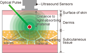
Photoacoustic imaging combines the propagation characteristics of ultrasound and the absorption characteristics of light into a new hybrid imaging method. By using ultrasound technology, it can obtain accurate information to a depth of several millimeters: hemoglobin selectively absorbs the energy of light and returns ultrasonic waves to the surface of the skin, where they can be captured by sensors. The information obtained can be displayed numerically and as a high-contrast map of blood vessels in the dermis.

microscope2

Principles of Photoacoustic Imaging

Advantest has been developing photoacoustic technology since 2010. The company’s independently developed sensors and electrical circuits permit high-speed measurement without exceeding the MPE (maximum permissible exposure) guidelines for exposure of skin to a light source. The new Hadatomo offers a measurement area of 4 mm × 4 mm × 3 mm (depth) and a maximum speed of 20 seconds per scan. Proprietary algorithms process the data obtained through dedicated software and construct 2D and 3D images in quasi-real time.

Find out more:

Read More

Posted in Featured Products

High Resolution TDR Error Detection for Advanced ICs

Short-pulse Signal Technology Enables 5µm Resolution Fault Isolation to Pinpoint and Map Circuit Defects

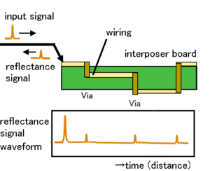
Electronic device circuit quality analysis is commonly performed using oscilloscope TDR (time domain reflectometry). However, as devices grow smaller and more highly integrated, the ability to locate failures with extreme spatial precision has become increasingly more important. Existing measurement instruments have limited resolution, as the rise time of the short pulse cannot be compressed much further, creating the risk that existing analysis technologies will be inadequate to handle the requirements of the highly integrated devices on the horizon.
Advantest’s terahertz analysis technology addresses these concerns and meets the need for ultra-high-resolution measurement and analysis of complex electrical circuits by utilizing short-pulse signal technology to enable 5µm resolution fault isolation to pinpoint and map circuit defects.

The company’s new TDR Option for the TS9000 series of terahertz analysis systems enables analysis of circuit quality in semiconductors, printed substrates, electronic components, and other applications, utilizing short-pulse terahertz waves.

ts9000

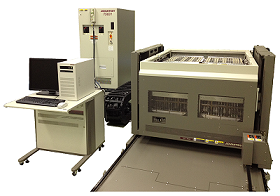
TS9000 TDR Option probe station

The TS9000 TDR Option relies on Advantest’s market-proven TDR/TDT measurement technology to pinpoint and map circuit defects utilizing short-pulse signal processing. The solution delivers circuit analysis with an extremely high spatial precision of less than 5µm, and a maximum measurement range of 300 mm, including for internal circuitry used in through-silicon vias (TSVs) and interposers. Moreover, with the optional TDR/TDT CAD Data Link, errors located can be mapped and displayed on the CAD data of the target device, making it much easier for users to identify the causes of errors. Three types of TDR/TDT probes, each with a different resolution and measurement distance setting, are available for the TS9000 TDR Option, as are customizations for unique contact requirements.

3d-semiconductor

ts9000-2

3D semiconductor wiring failures and TDR measurement examples

Find out more:

Read More

Posted in Featured Products

EVA100 Digital Solution Offers Design-Production Testing

Many IoT-enabled electronic products receive information in analog form, then convert it into signals for transmission. This requires the use of integrated digital ICs. These semiconductors are extremely cost sensitive, and the markets for them are highly competitive.  In addition, digital ICs are used in a wide range of applications, many of which impose stringent safety and reliability standards that put a premium on device performance and accuracy. For these reasons, producers of digital ICs typically employ high-mix, low-volume production methods, which require highly versatile and cost-efficient testing capabilities.

With its flexible architecture, Advantest’s new EVA100 Digital Solution can perform all of the functions needed for testing digital ICs, as well as pattern generation and comparison for evaluating device designs, digital control, power source measurements and 18bit analog measurements. It can conduct all of these measurements at 100Mbps data-transfer rates and up 200MHz clock speeds, resulting in high-efficiency testing.

EVA100 Digital Solution is the latest member in an expanding line of EVA100 measurement systems for testing a broad variety of digital ICs, including IoT devices, microcontroller units (MCUs), design-for-test (DFT) and built-in self-test (BIST) semiconductors and logic ICs. It is available in both production and engineering models, with capabilities that include design evaluation, front-end and back-end measurements, fault analysis, package verification and acceptance inspection of devices.

eva-100


EVA100 Digital Solution


eva-1002

Fully Integrated Digital Testing Needs

The new digital solution enables a customer to establish a common measurement environment throughout a facility, from design evaluation through production – achieving efficiency-boosting standardization that is unmatched by any existing measurement instrument or system. Furthermore, it is 40 percent smaller than the initial EVA100 measurement system, saving time and money by simplifying operation and making periodic maintenance much easier.  Scaling down the architecture also helps the EVA100 Digital Solution to deliver both high reliability and industry-leading productivity.  With each compact unit having a maximum of 256 measurement channels, as many as four EVA100 Digital Solutions can be clustered together to create configurations of up to 1,024 digital channels.  This enables the system to match manufacturing volumes with market needs by readily accommodating changes in production volumes and line retooling for different device types.  It also gives users the flexibility to optimize test environments for logic circuits and IoT devices, many of which utilize DFT.  Additionally, the measurement system can apply the same test programs for design and evaluation as for production, eliminating the need to change program codes and accelerating new devices’ time to market.

Find out more:

Read More

Posted in Featured Products

Simultaneous Measurement Solution for High-volume ICs

With market demand growing for price-sensitive ICs used in automotive, smart phone and other high-volume applications, conducting simultaneous measurements of multiple semiconductors has become vital to test cost reduction. Performing such highly parallel testing requires a performance board capable of handling the many circuit loads necessary for testing today’s most advanced analog devices.

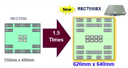
Ideally suited to this requirement is Advantest’s new RECT550EX HIFIX (High-Fidelity Test Access Fixture),  which enhances the capabilities of its T2000 system-on-chip (SoC) test platform in performing highly parallel testing With  50 percent more application space and a capability of handling 30 percent more channels than its predecessor, highly parallel and simultaneous measurements can now easily be attained.

The T2000 platform is capable of accommodating several high-density test modules in the test head. The RECT550EX HIFIX enables the T2000 to take full advantage of these modules by allowing the system to be configured as needed for any device under test (DUT), including automotive semiconductors and power-management ICs. In addition, the new HIFIX unit maintains full compatibility with Advantest’s standard RECT550 HIFIX performance boards. When equipped with the RECT550EX HIFIX, the T2000 SoC tester can achieve an extremely low cost of test.

Find out more:

Read More

Posted in Featured Products

Wireless Data Logger Revolutionizes Automotive Industry Processes

Advantest’s new AirLogger WM1000 is the widely anticipated wireless data logger for commercial applications. Compliant with FCC regulations and certified under the Technical Regulations Conformity System of Japan, the WM1000 has diverse uses in the automobile industry and beyond, from R&D to the production floor.

The AirLogger’s sensor unit, which incorporates a thermocouple data processor, wirelessly sends temperature data to a PC for display and saving. It can measure temperatures at 100 points, and can also measure the temperatures of moving and rotating objects, such as wheels, which are difficult to measure with existing temperature loggers. These capabilities give the AirLogger a wide range of applications in diverse sectors. The AirLogger has been praised by early adopters as a revolutionary instrument that cuts thermocouple setting time by 80%, and enables previously impossible temperature measurements of moving wheels and brakes.

In the automotive industry, and many other manufacturing and R&D fields, temperature measurement and evaluation are normally performed with data loggers whose measurement units and data processing units are connected by cables. Set-up, measurement, and breakdown take a considerable length of time, impacting process efficiency. Additionally, in recent years, measurement targets have become smaller, creating a need for smaller sensor units and simultaneous multiple point measurement functionality. Advantest’s AirLogger series addresses all of these challenges with its revolutionary wireless solution for temperature logging.

Customers adopting the AirLogger have seen dramatic productivity gains, as they are freed from the constraints of working with data cables.

airlogger

Key Features of the AirLogger:

  • Compact, Fully Wireless Design Dramatically Boosts Efficiency
    The AirLogger’s sensor units use button batteries for their power supplies and transmit temperature measurements wirelessly. The fully cable-free configuration enables dramatic productivity gains and enables easy temperature measurement for formerly difficult-to-measure targets such as revolving tires and other moving objects.
  • Real-Time Simultaneous Measurement of Temperatures at Multiple Points
    Temperatures at up to 100 separate points can be measured simultaneously, and measurements are processed in real time.
  • Fully Wireless Design Dramatically Boosts Efficiency

The AirLoggerTM’s sensor unit, which incorporates a thermocouple data processor, wirelessly sends temperature data to a PC for display and saving. The WM1000 dramatically boosts efficiency by freeing users from the constraints of working with data cables.

Find out more:

Read More

Posted in Featured Products

Die-Level Handling System Enables KGD Testing

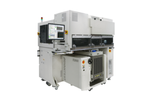
Advantest’s new HA1000 die-level handler is a cost-efficient test solution for determining known good dies (KGD) prior to IC packaging.  It is the ideal solution for high-growth applications including mobile electronics and high-performance networking devices.  With economics a driving factor in die-level testing, determining a semiconductor device’s viability prior to packaging or building memory stacks is critical to avoiding rework, achieving high yields and lowering costs.  The HA1000’s ability to perform pre-assembly testing of singulated devices provides a new level of visibility into the quality of the device prior to committing additional devices and expensive packages to an assembly that could potentially have to be scrapped because of undetected problems.

HA1000-1

The new die-level handler allows full device testing to be performed before assembly, providing time-critical information that typically is only available at final test.  HA1000 is designed to handle a wide variety of devices from large high-power server/GPU type devices to small systems-on-chip (SoCs) and memory devices/stacks, such as HBM2.   The die-level handler can accommodate both thick and thin parts as well as stacks of 3D devices and partially or fully assembled 2.5D integrations.   In addition, the HA1000 is ideal to probe fine-pitch pads, bumps, microbumps and pillars.  Future applications of the system may also include probing of through-silicon vias (TSVs).

When joined together with the V93000 test system, Advantest provides a full test solution called the Die-Level Tester (DLT). This solution offers the following capabilities:

  • Handles large, small, thick or thin devices.
  • Can handle 3D stacks, 2.5D assemblies, and even partial assemblies.
  • Vision alignment aligns the probes to pads, bumps, pillars or TSVs
  • Automatic planarity adjustments to insure solid contact to non-flat surfaces.
  • Integrated high-power active thermal control system to speed the testing of large complex designs.
  • V93000 provides the ability to debug and test high-performance digital, analog, RF, and DC devices.

HA1000-2

Target applications for the DLT reap a variety of benefits:

  • Probing the singulated die just before assembly can improve final product yield while greatly reducing the cost of scrap.
  • Active thermal control at the die level allows full final-test execution in order to maximize later yields.
  • The DLT allows full testing of previously untested devices that may have been delivered from a multi-project wafer.
  • The DLT performs KGD final testing of products to be delivered in die form.
  • The DLT can speed time to market by allowing detailed device debug while blind product build takes place.
  • The DLT can re-screen die-bank parts, allowing them to be re-programmed to meet new needs or tested to confirm performance to new requirements.

Most importantly, the handler’s precision vision alignment system precisely positions probe points to the finest pitch in use today.  While properly positioning the chuck under the probes, the system can also adjust the planarity to match with the device surface to ensure a solid device connection. Its active thermal control (ATC) system enables the HA1000 to adjust on the fly to temperature fluctuations at the die’s surface over a very broad dynamic range of -40˚ C to 125˚ C.  The temperature of the thermal head quickly responds using a hot-cold fluid mix.  Thanks to low thermal resistance and high thermal capacity, the system can handle high-power devices with a thermal responsiveness often better than is possible in a packaged environment.   This allows manufactures to test parts at higher power levels and/or tighter margins, which can improve yields while reducing scrap.

Find out more

Read More