Pages Menu
Categories Menu

Posted in Featured Products

T2000 IPS Solution for Power Device Testing

By Amit Monga, Business Development Manager, ASD Product Group, Advantest

Introduction

Integrated circuit devices that fall under the general power device category are getting more mainstream. The devices form an important part of a number of very fast growing industries including but not limited to the wireless, automotive and industrial industries. On the wireless side, PMIC devices are having significant growth as the need for battery management and LED driver integrated circuits grow. The automotive market sees a larger appetite for electrical components with safety (example: ABS, Power steering) and luxury (Example: infotainment systems) primarily driving this area of growth.

T2000 IPS Image1

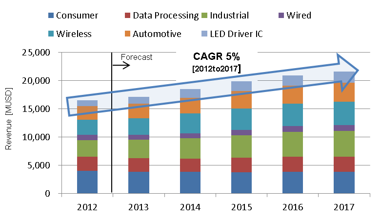
Source: Power Management Market Tracker – Q4 2013

Challenges and Complexity of Power Device Testing

As power device uses increase, so does the need to test them adequately. The wireless market, driven by smartphone and tablets requires device testing to be done at the lowest cost possible and yet the ever increasing integration of functionality in the devices means the IC has a lot more functionality. The average selling prices for the devices are very low and test budgets are limited. The test solution has to address this as well as ensure test quality is not compromised.

T2000 IPS image 2

The increasing integration poses a second challenge. The test demands are increasing. A few years back, power devices could be tested on a purely analog tester with a few power supplies. Now, a basic device requires some digital stimulation, high current and voltage requirements, and some are even integrating RF IP. Internet of Things (IoT) type devices are a perfect example of this increasing integration and complexity. Tester selection is therefore not based on a single device type but seen from a solution stand point. The selected platform should be scalable to accommodate the rapidly changing devices.

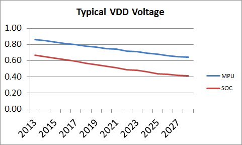
A general trend that is not particularly related to power devices but more to do with the shrinking process nodes is the decreasing supply voltages. This is especially true for wireless and consumer devices. PMIC devices such as the fuel gauge found in a number of smartphones are an example of devices that are required to monitor these voltage levels. This requires the chips to have very accurate voltage reading capability as well the ability to provide very precise biases. The capability is down to the sub 100uV range and test fixtures are having to redesign their modules to meet this challenge.

T2000 Image 3


DC Challenges:
Lower voltages,
More supplies,
Tiny power specs


The other challenges facing power device test are common across other family of devices. These range from minimizing test times, reducing time to market, maximizing parallelism and number of devices that can be tested at the same time and ensuring that the load board does not limit the parallelism. This is especially true for automotive power devices because each device requires a large number of on board components. The load boards that for other types of devices can test up to 64 or even 128 devices in one go suddenly seem inadequate for even 16 site testing of automotive parts. The major reason being the real estate available on the boards. Tester companies are aware of this and are continuously coming up with better module and load board design to counteract this.

The T2000 IPS Solution

The T2000 test platform is a scalable platform with modules that provide solutions for different device types and industries. The IPS solution refers to a particular set of modules that when populated into the T2000 tester, form a solution for power device testing. The modules provide a broad coverage and cover a whole range of different IC types.

T2000 Image 4

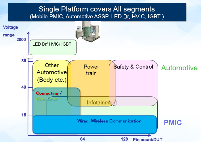
The T2000 IPS modules are designed to target some of the key challenges that power devices face during test.

T2000 Image 5

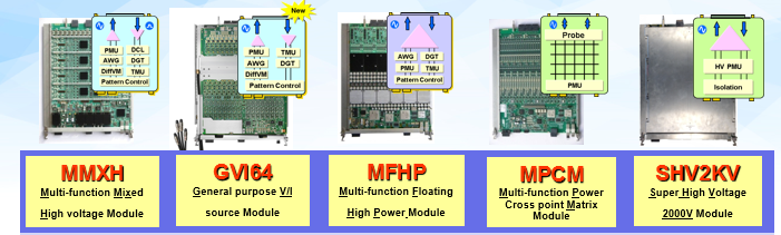
The modules have special multifunctional architecture (PMU, TMU, DGT, and AWG in one pin). This ensures that each module has a wide capability. This specially targets the increased complexity of devices, and ensures a large number of different tests can be handled by limited number of modules. The overall impact of this for power devices is not only a lower test system cost, but also having so much functionality per pin implies less load board space is wasted on relays. An Example of this would be a pin that for one test requires a PMU resource but for the next test requires a TMU resource. In addition, the MPCM module, a relay module that routes signals internally in the test head also leads to a reduction of load board relays. Overall in some cases this unique architecture has led to almost 40% reduction in the components on board as compared to conventional architectures.

The specifications on the MMXH PMU are also targeted towards PMIC and other devices that require high precision voltage source and measure. The solution has been successfully used with high precision Li-ion battery monitoring circuitry as well as band gap reference IC where stability and accuracy are key. In addition the modules provide high stability current measurement capability.

Some example test connections are shown below:

T2000 Image 6

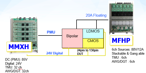
Automotive ASSP Device
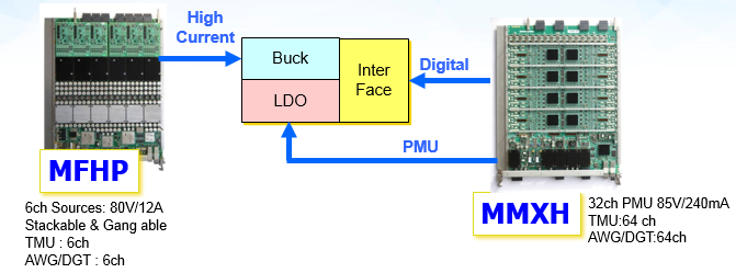


T2000 Image 7

PMIC Device

T2000 Image 8

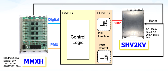
LED Driver IC Device


The other key advantage that the T2000 provides is the multisession architecture. This basically allows the tester to be accessed by more than one user and for more than one user to simultaneously debug tests online. This reduces the overall engineering development time and leads to much shorter time to market. The test modules are specially designed to take advantage of this architecture.

multisession architecture
Representation of multisession architecture

Summary

Testing of power devices for test solution providers has to be looked at from both a business and a technological point of view. Factors like time to market, cost of test, test time are key to making a business decision on the type of test platform but hand in hand, factors like device trends, accuracy, test coverage and stability weigh in. The T2000 IPS provides a comprehensive solution that targets both these selection criteria.

About the Author:

Amit Monga has a bachelor’s degree in Electrical Engineering from McGill University and an MBA from University of Toronto. He joined Advantest in 2006 as an application engineer and has experience in digital and analog SoC device testing. He is now part of the Business Development team at Advantest and focuses on developing strategies to address the power and image sensor test market.

Read More

Posted in Featured Products

W2BI Unveils SmartBox – an Innovative System Level Test Solution for Smart Device Testing

By Artun Kutchuk, Vice President, Business Development & Strategy, and Keith Schaub, Vice President, Corporate Development, W2BI, Inc., Advantest Group Company

Combining W2BI’s patented QuikStressTM Automated Smart Device Test Software with 3D Robotics

Smartphones and other smart devices are continuously integrating new functions. Many of these functions are physical movements (i.e. NFC, vibration, gyro, compass, accelerometer, temperature, and health / fitness to name a few). However, most test solutions today still target the non-physical aspects — the software, applications, RF and other specifications. As a backdrop to facilitate our discussion, let’s focus on three key life cycle segments of the smartphone:

  • Pre-Launch production testing
  • Post-Launch / Reverse production testing
  • Point-of-Sale / In store diagnostics and testing

Each of these life cycles are closely related in the types of testing and diagnostics performed. To highlight that, let’s talk about some problems Alex, Tim, and Vicky are having with their smart devices.

Alex recently purchased a new smartphone but is having some audio issues when listening to music on his headphones. Tim has had his smartphone for about 6 months and recently his touchscreen hasn’t been working properly. Sometimes his phone doesn’t register when he swipes or presses the screen. Lastly, Vicky has been missing important phone calls and finally discovered when in silent mode, the phone isn’t vibrating like it is supposed to.

I’m sure many of you have experienced similar problems. Typically, the first thing you would do is to take your phone back to the Point-of-Sale (store where you purchased it) and inform the store assistant of the problem. Now what? Well, the assistant asks if you can show him the problem. Sometimes you can, when it’s a hard failure, but often you can’t. It might be intermittent, or occur only after certain events, or it might be caused by a specific combination of interactions between the hardware, software, applications, etc. Some stores have software diagnostic tools that perform a gross health check, but often the problem or issue is scenario based, therefore the diagnostic tool typically won’t capture or flag the failure, so the phone gets marked as NFF (No Fault Found), or NTF (No Trouble Found). Conservatively, we’ve estimated that NFF/NTF classifications are costing the industry in the 100s of millions of US dollars, perhaps in the billions.

There are two main reasons for that. First, in the store, the assistant typically will swap out your phone, giving you a new phone, so already a few hundred dollars to give the customer a brand new phone. Second, the NTF phone then churns through the reverse production line where numerous tests are run at multiple test stations looking for the problem, when no fault is found, the phone gets wiped and resold as a refurbished unit. Someone has to pay for all that testing and refurbishing. There are entire 2nd and 3rd tier markets existing largely based upon the high quantity of NTF/NFF phones. So, it would be safe to say that it is a big problem when the problem itself subsidizes entire markets.

There is a rule of thumb in industry for an end-user:

  • In the first occurrence of the problem –> Change the phone
  • In the second occurrence of the problem –> Change the Operator

The first time a customer has a problem with his phone, the customer is annoyed, would most probably change the phone – get a new one or upgrade to a newer model. If the store had to send his phone to the repair center, then he is without his phone for several days.

Then second time he has a problem, now he is extremely frustrated. The operator didn’t fix it the first time, and now he has to go through this again, so there’s a very good chance that he will switch operators.

You might ask. Didn’t any of this get tested at pre-launch? In fact, yes, smart devices with their myriad of integrated functions including: audio, touch screen, video, FM, BT, WiFi, NFC, compass, gyro, accelerometer, etc.), literally require a small army of people manually testing each function. The testing is highly subjective and prone with human errors and each function is generally tested standalone – that is, non-scenario based. Additionally, the emerging Internet of Things (IoT) devices are further complicating testing with high mix and low volume complex test setups.

This has created a need for a new platform that is low cost, easy to use, and automated consisting of robotics, and system level software able to interact and test functions, user scenarios, mission modes, and applications.

At W2BI, we developed an innovative platform, SmartBox, that:

  • Functionally tests key components of a smart device at pre-Launch Production, Point of Sale (POS) and Repair Depots completely automated with typical end-user scenarios
  • Scales the features and functions appropriately for the three key market segments (i.e. Pre-Launch, Point Of Sale, Post-Launch)

w2bi-img2The Key Values & Benefits to customers

  • Reduce NTF/NFF
  • Isolate quality issues
  • Classify true failures
  • Eliminate subjectivity
  • Verify & validate repairs
  • Increase Customer Satisfaction

W2BI’s SmartBox platform combines robotics with system level software designed to be a low-cost scalable profile with a simple and easy to use experience for Production Testing, Point of Sale and Return Depot end users. All major functions as well as integrated applications and user scenarios can be tested automatically.

w2biIn addition to testing the software, OS, UI, applications, and user scenarios, SmartBox will be able to test the physical functions, namely:

  • Touchscreen
  • Audio / Video
  • Camera / Lights
  • Vibration
  • Accelerometer
  • Physical Buttons
  • Compass
  • NFC / Wireless Charging
  • Gyro
  • Temperature
  • Health & Fitness

With SmartBox:

  • Point of Sale: A store assistant can potentially place the smartphone inside, chose one or more tests including scenarios and within a few minutes get back a non-subjective actionable assessment.
  • Pass/Fail result. Reverse Logistics / Repair Centers: Quickly and easily verify a failure as well as verify a successful repair and eliminate subjective errors caused by manual testing.
  • Pre-Launch Production: Automatically test and verify all of the physical functions eliminating manual labor and human error.

About the Authors:

Artun Kutchuk has over 25 years of experience in wireless, aerospace, robotics, business process automation and software development. He holds an M.Eng. Degree from McGill University. Artun also has co-founded a start-up and holds several patents in mobile device testing and diagnostics. Prior to W2BI-Advantest, Artun held multiple positions at Carrier IQ, Ericsson, Interfacing Technologies and CAE.

 Keith Schaub has worked in RF & Wireless Semiconductors for more than 20 years. Keith is the author of Production Testing of RF and System-On-a-Chip Devices for Wireless Communications. He holds five patents on various wireless devices and test systems, founded two start-ups, and is an avid writer and publisher on wireless topics.

Read More

Posted in Featured Products

T5833 Memory Test System

T5833---150604_044To keep pace with users’ performance demands in the booming market for mobile electronics, the semiconductors that drive smart phones and tablet computers as well as the servers that support them – primarily DRAMs, NAND Flash memories, multi-chip packages (MCPs) and next-generation non-volatile memories including MRAM, RRAM and PCM — are becoming faster and higher capacity. This raises the need for test solutions that have both the high functionality to test today’s most advanced memory ICs and the cost-efficient operation to address high-volume consumer markets.

The versatile T5833 memory test system combines industry-leading performance and low cost of test to maximize customers’ return on investment. The tester is designed to perform both wafer sort and final test across a wide range of memory devices including LPDDR3-DRAMs, MCPs, high-speed NAND flash memories and next-generation non-volatile memory ICs.

https://www.advantest.com/news?articleId=295719

Read More

Posted in Featured Products

DPS128

DPS128angle
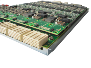
One of three new modules recently launched in support of the V93000 test platform with universal per-pin architecture, the DPS128 (device power supply) is part of a family of power-supply instruments designed to provide a cost-efficient response to the trend toward higher multi-site parallelism. The DPS128 features 128 channels of voltage/current (VI) resources per module to accurately source and measure both current and voltage. Its modular architecture, based on Advantest’s test-processor backbone, can be configured in multiple ways. This built-in flexibility and expandability is key to the power supply’s ability to meet future testing needs.

The DPS128’s per-pin time measurement unit (TMU) enables efficient measurement of high switching frequencies, duty cycles and fast rise/fall times found in today’s advanced power-management devices. With its sophisticated ganging options, this family of instruments can address a broad application space, and also supersedes legacy power instruments within the V93000 portfolio.

This new product family has been instrumental to the growing success of the V93000 in the microcontroller, smartcard, sensor and automotive segments, because it enables very small and attractive system configurations (few cards) with high versatility.

SoC customers have widely accepted the new instruments, and Advantest shipped roughly 1,500 units within the first year. This steep ramp is a first in the history of the V93000 platform. The majority of the units are meeting the high-volume production needs of customers located in Asia.

The products in the DPS family set a new milestone in versatility and cost efficiency, and Advantest looks forward to seeing them contribute further to our growing SoC business.

DPS128

Read More

Posted in Featured Products

PVI8

PVI8
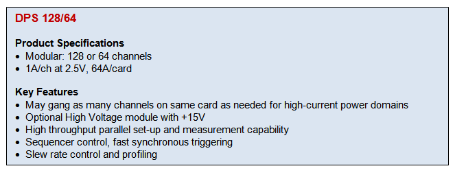
In 2014, Advantest announced its new PVI8 floating power source for the V93000 universal per-pin test platform. The new instrument adds high-voltage and high-current test capabilities to Advantest’s universal V93000 platform, and broadens its market to embedded power devices. Typical target applications in this area are motor controller ICs for automotive and industrial usage and a broad range of power-management devices, including high-power buck and boost converters.

The PVI8 features high channel density and lower test time compared to competitive systems. Designed with eight floating channels and four-quadrant operation, the new instrument can be used to provide up to 80 volts and up to 10 amps per channel. The eight-channel PVI8 can be ganged up to ±80 amps for high-power stress testing of devices. For high-voltage tests, the PVI8 can be stacked up to ±160 volts due to its floating design. The power source supports native pattern controlled operation and therefore leads to extremely fast test times with stable parametric measurements.

Current customers for the PVI8 are leading IDMs in the automotive area. One of these IDM customers is using the power source to test a series of embedded Power MCUs for automotive body electronics. The high channel density, rich feature set and high-throughput of the V93000 power solution provides compelling test cost for embedded power devices.

Efficient test development is essential for these complex applications to meet their short time-to-production requirements. A software package for automatic creation of high-throughput-pattern controlled setups and measurements enables the creation of high-throughput test solutions with reduced engineering effort.

For more information, visit Advantest.com.

PVI8-specs

Read More

Posted in Featured Products

TS9000

Growing global adoption of smartphones and tablets with thin form factors is driving demand for semiconductor devices to be smaller and more highly integrated. Extremely precise mold thickness management is necessary for these cutting-edge semiconductor processes. However, quality management in the molding process has been challenged by the fact that non-destructive mold thickness measurement tools were not available, meaning that engineers must extract individual device samples during the trim and form process, cut them destructively, and inspect the cross sections by microscope. This is a time-consuming process typically involving a long wait time due to a bottlenecked queue.

TS9000
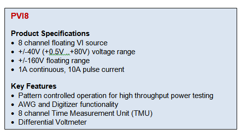
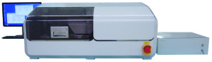
Advantest’s TS9000 Mold Thickness Analysis (MTA) System solves these issues by utilizing terahertz waves to measure mold thickness non-destructively, rapidly, and with a high degree of precision. The system’s high throughput enables users to test large volumes of samples and readily grasp the mold thickness distribution of entire lots. For the first time, users can inspect mold thickness during volume production.

The TS9000 works by placing the semiconductor devices to be measured on the measurement unit’s XY stage. It rapidly evaluates multiple “measurement points” and analyzes the mold thickness distribution. By re-using files containing sets of measurement points (“recipes”), the system can easily inspect devices of the same type without reprogramming. During measurement, it can display thickness measurements and reflection waveforms from each measurement point in real time. These data are recorded in files for each production lot, and can be used for online data management.

The system over­comes the limita­tions of traditional measurement methods by enabling repeatable and highly accurate measurements, even when analyzing the opti­cally opaque mold polymer materials typically employed in circuit packages. It can handle die in strips or singulated units and is also fully compatible with industry-standard JEDEC trays. During testing, the display shows the status of samples being analyzed along with other important information, allowing the operator to fully monitor test progress.

Fully non-contact and non-destructive, the TS9000 can be configured for partial or 100-percent inspection of the product. Analysis points are fully user defined, ranging from one to 20 points per unit. In addition, the system is fully adaptable for use at various points in the assembly and packaging process, including earlier stages where it can improve product quality and yield.

For more information, please email THz_info@advantest.com or visit Advantest.com.

Read More