Pages Menu
Categories Menu

Posted in Featured Products

Advantest Targets NAND Flash/NVM Market with New Group of Memory Test Products

In December, Advantest announced three new additions to its suite of memory test products. The new offerings are designed to target NAND Flash and non-volatile memory (NVM) devices, which face extreme pressure to bring down test costs and cost of ownership on the test floor. The new products include the T5230 memory wafer test solution; the STM32G third-generation protocol NAND system-level test module for the T5851 memory tester; and the T5835 high-speed wafer-sort interface option.

The T5230 memory test system for NAND/NVM devices adopts a combined array architecture to achieve best-in-class cost-of-test performance for wafer test, including wafer-level burn-in (WLBI) and built-in self-test (BIST). The system can perform on-wafer test of 1,024 memory devices per test head in parallel, delivering high productivity and enabling floor space savings of up to 86%. Multiple test cells are connected per system controller in the T5230, allowing independent wafer test of each test cell. The test cells can be stored in a general multi-wafer prober while minimizing the test cell floor space, and the tester can be docked with probers in both linear and multi-stack configurations. For functional tests at a maximum test rate of 125MHz/250Mbps, the T5230 assures high timing accuracy, repeatability, and failure detection capability.

T5230 Memory Test System

The T5851-STM32G module is designed to cover the latest generation of protocol NAND devices, including UFS4.0 and PCIe Gen 5 ball grid array (BGA) packaged devices for high-speed system-level NAND testing at up to 32Gbps. Fully upgradeable and compatible with existing T5851 systems, the new module delivers tester-per-DUT (device under test) performance and is qualified for high-volume manufacturing, qualification, reliability and characterization.

T5851 Memory Test System and T5851-STM32G

Created as an option for the proven T5835 multifunction memory test system, the new high-speed wafer-sort interface enables high-speed NAND Flash/NVM wafer probing (up to 5.4Gbps) with 4,096 full I/O channels. Raw NAND die inside solid-state drives (SSDs) require increasingly higher-speed functionality, necessitating evaluation and test of die performance at the wafer level, not just in package-level final test. The solution delivers high-speed probe interface with wafer-level evaluation of memory core test functionalities during engineering production, contributing to the T5835’s overall value by delivering wider test coverage.

T5835 Memory Test System


Read More

Posted in Featured Products

Advantest Rolls Out Pin Scale Multilevel Serial – Next-Generation High-Speed ATE Instrument

In November, Advantest announced the Pin Scale Multilevel Serial, its newest high-speed I/O (HSIO) instrument. Designed for use with the V93000 EXA Scale ATE platform, Pin Scale Multilevel Serial is both the first native EXA Scale HSIO instrument and the first fully integrated HSIO ATE instrument to address signaling requirements for advanced communication interfaces.

HSIO interfaces, long prevalent in the computing space, have found their way into consumer interfaces such as HDMI®, DisplayPort™ and USB. In the computing space, PCI Express (PCIe) 5.0 and 6.0 are entering the multi-gigabit data-rate range and being leveraged in embedded single-board computers. Companies testing large digital designs and their interfaces, from microcontrollers and mobile application processors to high-performance computing and artificial intelligence (AI) devices, require HSIO to accommodate these high-density designs. HSIO testing is thus vital for the characterization of these new device designs as well as for early device manufacturing ramp phases. 

Pin Scale Multilevel Serial supports data rates up to 32 gigabits per second (Gbps) and is the first fully integrated ATE instrument that natively supports multilevel signaling (e.g., PAM4), which is rapidly growing in high-speed interfaces. This heightens ease of use as it enables the use of programming schemes typical in digital test, reducing test program development time and cost. As such, it helps to optimize leading-edge technologies and speed time to market by providing additional test coverage for ramping of new chip designs. 

Because Pin Scale Multilevel Serial is fully integrated, it can be easily configured into the EXA Scale platform. Competitive offerings typically require an integration stage to be mounted between the top of the test head and the interface to the device under test (DUT), degrading signal performance and worsening manufacturing integration. 

Read More

Posted in Q&A

Interview with Linda Haenel, VOICE 2024 Chairperson

By GO SEMI & Beyond Staff

Advantest’s VOICE 2024 Developer Conference will take place June 3-5 at the Hilton La Jolla Torrey Pines in San Diego, California. To learn what VOICE 2024 holds in store for attendees, we interviewed this year’s general chairperson, Linda Haenel, application consultant, Performance Digital Center of Expertise, Advantest Europe.

Q. With VOICE 2024 taking place in San Diego, how will this year’s location impact the event?

A. San Diego holds great importance for our industry. We anticipate large attendance at this year’s event due to the significant local presence of major semiconductor companies such as Qualcomm, NXP, and Infineon, as well as the location’s relative proximity to Silicon Valley. Also, with the Semiconductor Wafer Test Conference also being held June 3-5 at the Omni La Costa in Carlsbad, we will likely experience some cross-traffic between SWTest and VOICE. We are thrilled to be hosting VOICE at a location that is both accessible and beautiful, with this year’s venue nestled alongside the California coast, offering breathtaking views of the Pacific Ocean.

Q. As the VOICE 2024 chair, what would you hope to see, or what would you hope attendees will gain?

A.  As they do every year, the members of the VOICE committee work hard to offer a memorable event where industry experts come together to share information, learn, collaborate, and network. I want each attendee to come home with something – a new thought, idea, or contact that will inspire them. We’ve built VOICE to be a platform that fosters the exchange of great ideas, leading to the innovations that propel our industry forward, “beyond the technology horizon.” We’ve adopted this theme once again because it is so descriptive – VOICE has always strived to deliver a glimpse beyond that horizon, through test experts’ papers, panels and kiosk presentations, to future advancements.


Q. This year marks Advantest’s 70th anniversary. What does this milestone mean to VOICE?

A.  In many ways, VOICE is emblematic of the relationships Advantest has developed over the past 70 years that have led us to where we are today. Many of the companies participating have worked with Advantest for decades, developing creative products and innovations that pioneered new standards for our industry. We are incredibly grateful to celebrate this milestone with them, and we’re excited to think about what the future, and our 100th anniversary, will bring as we continue to work closely together. 

Q. What are some of the hot trends and topics for 2024?

A.  Our committee accepted more than 100 technical papers this year – a new VOICE record. These papers are distributed over nine technical tracks, and we expect Test Methodologies, High-Performance Digital, and 5G/Millimeter Wave to be featured significantly during the technical sessions.

We are excited to introduce a new Artificial Intelligence (AI) track for VOICE 2024. This track will examine how engineers can benefit from utilizing AI applications in semiconductor production test for data analysis. Papers will also explore how our industry can utilize AI applications in test engineering to streamline test program development. 

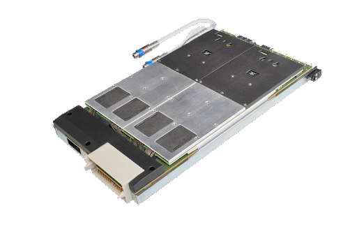
There will also be presentations showcasing Advantest’s new Pin Scale Multilevel Serial for the V93000 EXA Scale platform. Released last year, this new product is both the first native and fully integrated HSIO instrument that expands the EXA Scale platform to address signaling requirements for advanced communication interfaces. The card’s multi-level capability enables new signaling schemes emerging in HPC/AI and consumer markets, supporting NRZ and PAM4. 

Q. What highlights of this year’s event do you recommend attendees not miss?

A.  As always, there is much to look forward to. The conference will begin with a welcome reception on Monday evening that will offer a valuable opportunity to network with representatives from leading semiconductor companies. Concurrent with the reception, we will host the Technology Kiosk Showcase, which will include inspiring displays of the latest innovations that leverage Advantest’s broad product portfolio.

Tuesday and Wednesday will feature engaging keynotes from semiconductor market analysts and leading professionals. The Partners’ Expo is also open throughout Tuesday and Wednesday, allowing attendees to engage with our technology partners to discuss their latest products and solutions. 

I am especially excited for Tuesday’s evening event that will take us to the Birch Aquarium, where attendees will enjoy a lovely evening dinner alongside exhibits featuring tropical fish, Leopard Sharks, giant kelp forests, and Little Blue Penguins. The Birch Aquarium is associated with the University of California San Diego’s Scripps Institution of Oceanography and, much like Advantest, maintains a strong commitment to sustainability and local conservation efforts. We look forward to learning more about how we can preserve our oceans and the unique wildlife that lives beneath the surface. 

We will close VOICE 2024 on Wednesday afternoon with an award ceremony celebrating the best papers and honorable mentions. We will also give out the Visionary Award, presented annually to a customer who has made significant, sustained contributions to VOICE over a long period.

Q.  Who will be joining us for this year’s highly anticipated keynote addresses?

A.  I am pleased to announce that VOICE 2024 will feature three dynamic keynote speakers.

Our first speaker, on Tuesday, will be Craig Nishizaki, vice president of the Test Solutions Group at NVIDIA, which is responsible for providing manufacturing hardware and software test solutions for all NVIDIA’s products, from chips to boards to servers. 

Our second Tuesday keynote will be delivered by Marcelo Ackermann, professor, XUV Optics Group at the University of Twente (Netherlands), and chair of the Industry Focus Group – X-ray and EUV (XUV) optics at the university’s MESA+ institute. As a professor, he focuses on the development of next-generation reflective, refractive and transparent X-ray and EUV optics in collaboration with industry partners like Zeiss, ASML, and Malvern Panalytical. 

Wednesday’s keynote will be presented by Andrea Lati, director of market research at TechInsights. For more than two decades, Andrea has managed and developed forecasting models as well as performed market analysis and research on electronics, semiconductor, and equipment markets for TechInsights.

As a final note, we would like to thank our VOICE 2024 sponsors for making this year’s event possible—in particular, our headline sponsors, ISE Labs, ASE Group and Alliance ATE Consulting Group. The full list of sponsors can be found here.

To learn more about keynotes, papers, and other details related to VOICE 2024, be sure to keep checking the VOICE website. And don’t forget to register here to reserve your spot!

Read More

Posted in Top Stories

The Future of Data Analytics and Semiconductor Testing

This article is adapted with permission from a recent Advantest blog post.

By Michael Chang, Vice President & GM ACS, Advantest

The world is changing more rapidly than ever. With the explosion of Artificial Intelligence (AI), Machine Learning (ML) and data analytics, semiconductor manufacturers now have the opportunity to extract valuable insights from the massive amounts of data being generated throughout the silicon lifecycle. By leveraging AI algorithms and ML, semiconductor manufacturers can now optimize silicon design, assembly, and testing processes. It is through the analysis of these vast amounts of data, AI can quickly identify patterns, predict failures, and optimize quality. 

So, what does this all mean? It means that we now have the capability to greatly improve yield rates, reduce production costs, and accelerate time-to-market. Ultimately, the goal is to create an end-to-end utilization of analytics throughout manufacturing and test operations so that data analytics and ML will enhance the speed and accuracy of the testing process, reduce the risk of defects, and help the entire industry move ever closer to its goal of zero defects.  

This is where Advantest is revolutionizing the test industry. We just announced Advantest’s ACS Real-Time Data Infrastructure (ACS RTDI™), a solution that offers advanced analytics, including machine learning capabilities and future-proof, real-time, automated production control. The Advantest ACS ecosystem integrates all data sources across the entire IC manufacturing supply chain, a revolutionary first in the industry. In fact, ACS has been collaborating with multiple major data analytics companies as part of an industry-wide collaboration to accelerate data analytics and AI/ML decision-making within a single, integrated platform. These partnerships will help customers take advantage of new levels of data integrity and security across different test nodes and benefit from proven infrastructure solutions that will enable them to achieve new levels of operational efficiency. 

This is how Advantest is unlocking the intrinsic value of AI in semiconductor testing. 

The ACS RTDI platform integrates data sources across the entire IC manufacturing supply chain while employing low-latency edge computing and analytics in a secure True Zero Trust™ environment. This innovative infrastructure minimizes the need for human intervention, streamlining overall data utilization across multiple insertions and supporting customers’ databases. Because security remains a top concern among customers, the ACS RTDI platform has been architected to be reliable and safe, ensuring hassle-free OS revisions, while protecting data from unauthorized access or loss. This is accomplished by leveraging True Zero Trust™. Overall, the new ACS ecosystem will enable customers to boost quality, yield, and operational efficiencies, and to accelerate product development and new product introductions for years to come.

To fully support ACS’s revolutionary strategy, we also offer the ACS Solution Store which enables customers to choose from a comprehensive collection of software solutions designed for the digital age, addressing major challenges facing the semiconductor industry and that can be tailored to individual customer needs. Customers can select from the ever-expanding catalog of solutions in an easy-to-navigate browsable online catalog ― from a growing list/ team of partners joining the Advantest open solution ecosystem revolution.

Figure 1: Semiconductor Integrated Workflow and Benefits

Learn more about how Advantest is improving the technological world by setting a new standard in the semiconductor industry on our website: https://www.advantest.com/acs/overview/.

Read More

Posted in Top Stories

Solving High-Energy Testing Challenges

This article is a condensed version of an article that appeared in the November 2023 issue of Electronic Specifier. Adapted with permission. Read the original article here, p. 12.

By Fabio Marino, Managing Director, CREA, an Advantest company

Although the global semiconductor market is currently experiencing a slowdown, the automotive sector remains solid fueled by the demand for EVs. What used to be a niche market is now rapidly expanding to the mainstream, and companies that supply power IC technology must increase production volume to meet growing demand. 

Last year, CREA leased a new building to expand production capacity and keep up with ongoing business growth. This will allow CREA to produce test equipment for a wide variety of power semiconductors, including insulated-gate bipolar transistors (IGBT) and silicon carbide (SiC) and gallium nitride (GaN) semiconductors. SiCs’ advantages over traditional IGBTs include higher thermal conductivity, better ability to tolerate high voltages, higher switching speeds and lighter weight. Wide-bandgap technology such as SiC is the key to developing more efficient advanced battery systems that will enable new electric vehicles (EVs) to go farther and faster. 

Addressing high-power test requirements

Parasitic inductance and capacitance, which play an important role in the measurement, can create conditions that may damage the tester. Thus, testing high-powered SiC devices requires highly refined, specialized test equipment. CREA’s low-stray-inductance and probe card interface (PCI) technology enables engineers to minimize parasitic values. This allows the performance of specialized tests needed to ensure reliability and quality, facilitating the development of efficient batteries for new EVs. 

To meet customer demands for lower cost, CREA is expanding its bare-die test capabilities. Bare-die test utilizing the PCI and thermal control technology holds the key to expanding dynamic test to the wafer level. Package test is simpler, but if a single switch malfunctions, the entire package must be discarded. Bare-die test is more cost-efficient and creates less waste—the only challenge is that a probe card is needed to perform the test. Probe cards are fragile, and the high amount of energy generated during dynamic test can break the probe card and damage the tester itself.

CREA’s PCI technology monitors each probe needle for abnormal current distributions, shutting off the tester when such an abnormality is detected to prevent damage. CREA also developed a chamber for bare-die test that moderates temperature by controlling airflow to prevent sparking that can occur while working with high voltages, ultimately reducing the threat of harm to the ATE.

SiC technology provides many benefits over traditional IGBT technology, as noted earlier. While many major semiconductor companies are investing in R&D to support SiC technology, SiC is very different from silicon wafer technology. It requires completely different equipment, and the automated tools that factories currently have are designed for silicon wafers and will not work with SiC. Because SiC is a maturing technology, production yields are low. This creates a significant opportunity for test companies to deliver SiC-optimized test equipment. CREA continues to refine its power IC testing technology to increase yield and help customers maintain sustainable business models that can keep up with rising demand.

Conclusion

Fueled by major investments from the global semiconductor community, the power IC industry is evolving quickly. This creates significant opportunities for companies like CREA that are building solutions to address high-power specs and overcome industry challenges.

CREA’s patented LSI™ and PCI™ technology provides specialized testing solutions for power ICs found in hybrid and EV automotive engines. These solutions will accelerate the shift from 400V to 800V batteries, accommodating the testing specs needed to develop cutting-edge EV technology. Today, CREA engineers are developing techniques to run high-energy tests in parallel – increasing yield and helping to accommodate rising global demand for SiC and other advanced power semiconductors. 


CREA’s Power Device Testers

Read More