Pages Menu
Categories Menu

Posted in Top Stories

Concurrent Measurement on Wave Scale RF8 Enables Wi-Fi 7 EVM Test Improvements

By Joerg-Walter Mohr, Product Definition Expert, Advantest Corp.

The November 2022 issue of GO SEMI & Beyond included an article detailing how Advantest has evolved our Wave Scale family of test cards for the V93000 test platform by readying Wave Scale RF8 to address the test challenges associated with the forthcoming Wi-Fi 7 standard. This article provides further details on how to augment the Wave Scale RF8 solution by putting an additional splitter on the load board. With this splitter, two RF measurement systems can be used concurrently/simultaneously to improve the EVM measurement of one DUT RF signal.

The Wi-Fi 7 standard covers the now less congested frequency range between 6 GHz and 7.125 GHz, which was opened as an extension to Wi-Fi 6 and called Wi-Fi 6E. Wi-Fi 7 utilizes this wide 6 GHz Band with channel bandwidth up to 320 MHz and going up to 4096 Quadrature Amplitude Modulation (QAM) schemes.

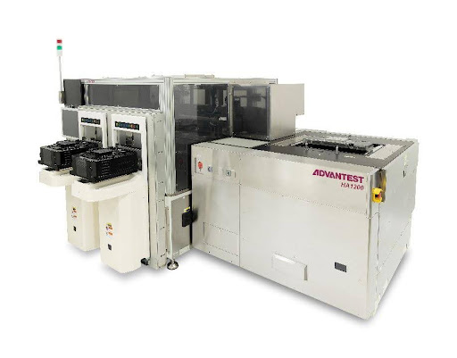
The Wave Scale RF8 solution addresses the test challenges associated with Wi-Fi 7 by providing the frequency range and the bandwidth needed in an industry-proven instrument (Figure 1). 

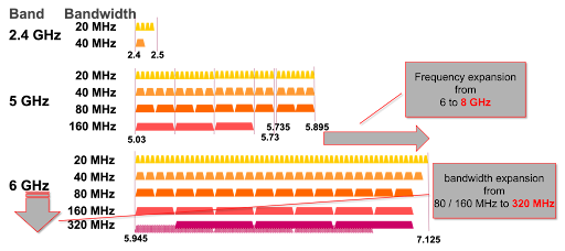
Figure 1.  Wave Scale RF8 enables measurements that fully address the frequency and bandwidth expansions associated with the Wi-Fi 7 standard.

The Error Vector Magnitude (EVM) of the modulated/demodulated symbols is an important figure of merit to describe the signal fidelity. EVM is measured either in % or in dB, where dB is used for smaller values for better readability. Wi-Fi 7 standard allows device transmitters to reach an EVM of -38 dB at most. Thus, devices will have better specs and production test equipment must be able to check those, e.g. -41 dB must be checked, which means test measurement unit should provide at least an EVM test capability of -44 dB if the device has a 3dB margin. Of course, for characterization purposes it is desired to have a test measurement unit with an EVM better than -50 dB.

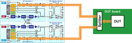
Figure 2.  Wave Scale RF8 concurrently measures with two RF subsystems one DUT Tx signal by adding a splitter on the load board.

Wave Scale RF8 EVM measurement performance can be improved by putting an additional splitter on the load board to enable the use of two RF subsystems simultaneously, as shown in Figure 2. By evaluating for each demodulated symbol the EVM, which is commonly detected by both RF subsystems, and neglecting the individual contributions to EVM of each RF subsystem, -50 dB EVM measurement capability is enabled for Wi-Fi 7 160 MHz 4096 QAM as shown in Figure 3.

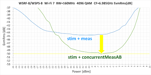
Figure 3.  EVM concurrentMeasAB test -50 dB for highest carrier frequency of Wi-Fi 7 160 MHz. Result with and without splitter for 160 MHz plus common error.

The reduced dynamic range due to the loss via the splitter can be compensated for by averaging in cases where the focus of the test is the detection of impairments caused by non-linearities. With averaging even for Wi-Fi 7 320MHz -50 dB EVM test capability can be achieved as shown in Figure 4.

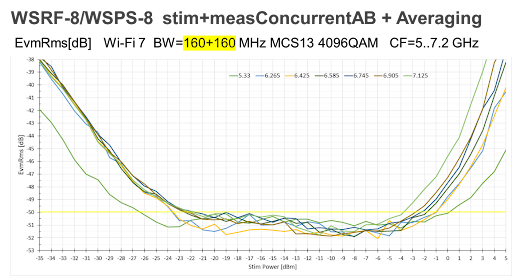
Figure 4.  EVM concurrentMeasAB + averaging test -50 dB for different frequency of Wi-Fi 7 320 MHz.

Summary

Using the high parallelism of the Wave Scale RF8 together with advanced test method addresses higher test requirements of the new standards like Wi-Fi 7 in the sub 8GHz frequency range. This might even be true for some upcoming FR3 applications in 5G/6G bands.

Read More

Posted in Uncategorized

2024-2025 Semiconductor Industry Outlook with TechInsights (Podcast Season 2, Episode 12)

Prepare to be illuminated by the insights of Risto Puhakka from TechInsights as he joins us to map out the semiconductor industry’s explosive growth, driven by the thunderous influence of AI. 

During our adventure through CES 2024, we bear witness to AI’s pervasive touch, from robotics and healthcare to the sizzling innovations in micro LED technology. Risto’s expert analysis doesn’t just skim the surface; it plunges into the economic, political, and competitive undercurrents that are redefining the semiconductor landscape.

Venture further into the conversation as we unravel AI’s sprawling web, extending its reach from agriculture to retail, and sculpting the semiconductor market’s future. We dissect the burgeoning world of spatial computing, and the surging demand for data streams, processor aptitude, and memory. 

Gaze into the crystal ball with us as we reflect on 2023’s rollercoaster ride – spotlighting industry bottlenecks and breakthroughs – and cast our predictions for 2024’s market climate. 

It’s not just a tech talk; it’s a strategic analysis of the global shifts, the CHIPS Act’s ripples, and how different nations are vying for supremacy in the AI arena. With Risto’s guidance, we’re decoding the blueprint of tomorrow’s semiconductor industry, where AI reigns supreme.

You can find this episode and more at this link: https://advantesttalkssemi.buzzsprout.com/1607350/14428141-2024-2025-semiconductor-industry-outlook-with-techinsights

Read More

Posted in Upcoming Events

Advantest Concludes Successful SEMICON Japan 2023 with Record Attendance

Advantest displayed its latest products and solutions at SEMICON Japan 2023, held on December 13-15 at the Tokyo Big Sight. As a result of Japan’s efforts to bolster its domestic semiconductor industry, this year’s event saw a significant increase in attendance from 50,000 people last year to 85,000 people this year. Advantest’s booth saw a 50% increase in booth attendance compared to last year, with a steady flow of visitors including customers, government officials, media personnel, and financial experts. 

Unlike previous years, Advantest’s 2023 booth featured an application-centric display, highlighting major applications like High-Performance Computing (HPC), Automotive, and 5G. Our new application-based approach helped us to connect with visitors from diverse backgrounds and showcase the crucial role our test technology plays in developing the world’s most cutting-edge applications. Our display included new products, such as the HA1200, ATC 2.0, Pin Scale Multilevel Serial, and the T5230 memory test system, demonstrating how our extensive product portfolio enables global innovation.

As a gold sponsor, Advantest sponsored various aspects of this year’s event including the APCS (Advanced Packaging and Chiplet Summit), Smart Mobility pavilion, and SuperTHEATER where President Yoshida-san gave a compelling speech on how Advantest is enabling the future with semiconductor testing. Additionally, Senior Director, Test Strategist of SVC Marketing & Business Development Shinji Fujita presented, “Challenges in Testing Advanced Large-Scale SoC Devices” during the SEMI Technology Symposium (STS). 

Thank you to everyone who contributed to the success of SEMICON Japan 2023! We look forward to next year’s event.

Smartphone and OTA sockets were displayed in IoT/5G corner, as well as QR & robotic arm demo


HA1200 in AI/HPC corner


Read More

Posted in Featured Products

Advantest Launches Real-Time Data Infrastructure (RTDI™) Platform Driving the Next Generation of Semiconductor Test

At the end of last year, Advantest announced that its newly launched ACS Real-Time Data Infrastructure (RTDI™) has been accepted by multiple major data analytics companies as part of an industry-wide collaboration to accelerate data analytics and artificial intelligence (AI)/machine learning (ML) decision-making within a single, integrated platform.

Advantest formed ACS in 2020 with the mission of enabling an open solution ecosystem data platform. ACS RTDI is a real-time data infrastructure that securely collects, analyzes, stores and monitors semiconductor test data to empower customers to automate the process of converting insights into actionable test decisions within milliseconds. This helps customers and partners reduce test time, optimize quality and reliability and enhance smart packaging.

“Advantest’s ACS RTDI platform turbocharges decision-making on test floor, while freeing test engineers from the tedium of having to search for needles in data haystacks,” said G. Dan Hutcheson, vice chair and senior fellow, TechInsights. “It lowers test cost with real-time test vector optimization while lowering packaging cost by shifting left systematic final test failures to probe.”

The ACS RTDI platform integrates data sources across the entire IC manufacturing supply chain while employing low-latency edge computing and analytics in a secure True Zero Trust™ environment. This innovative infrastructure minimizes the need for human intervention, streamlining overall data utilization across multiple insertions and supporting customers’ databases. Because cyber security remains a top concern among customers, the ACS RTDI platform was architected to be reliable and safe, ensuring hassle-free OS revisions, which protects data from unauthorized access or loss by leveraging True Zero Trust. Overall, the new ACS ecosystem will enable customers to boost quality, yield, and operational efficiencies, and to accelerate product development and new product introductions for years to come.

Read More

Posted in Featured Products

Advantest Expands Device Handler Offerings

In December, Advantest announced two new products designed to deliver advanced handling capabilities essential for the fast-growing artificial intelligence (AI) and high-performance computing (HPC) markets: the HA1200 die-level handler and the active thermal control (ATC) 2-kilowatt (kW) option for the M487x handler series. AI/HPC ICs require 2.5D/3D advanced packaging technologies to provide the high computing power necessary to generate, train and run data-intensive AI models. These ICs generate massive heat due to their high compute power, creating unique testing challenges. The new Advantest products are designed to address these challenges and help contribute to the AI/HPC market growth.

The HA1200 die-level handler for the V93000 SoC test system tests singulated and/or partially assembled die. While 2.5D/3D packages enable high computing power by enabling minimum pattern length between die, stacking die can increase the risk of mixing good and bad die, leading to yield loss. Yield loss at final test, especially for 2.5D/3D packaged ICs, can cause good die, substrates, or interposers to be discarded. Equipped with Advantest’s HPC-proven ATC technology, the HA1200 enables testing powerful, high-performance SoCs with 100% test coverage. This helps reduce yield loss at final test, thus reducing loss of final multi-die assembled product.

HA1200 Die-level Handler

The ATC 2kW solution for the M487x series (M4171, M4871ES and M4872) is designed to test AI/HPC IC packages at final test. The ATC 2kW solution features ultra-high-speed junction temperature (Tj) sensing and response technology to support high-performance ICs being tested at the set temperature and integrates Advantest’s unique force control technology to apply strong, stable, and safe contact to ICs with massive pin quantities. The ATC 2kW solution will support customers’ at-speed device test, enable safe 100% test coverage at final test while simultaneously increasing test quality and performance.

Read More