Interview with Artun Kutchuk
 W2BI, Inc., an Advantest Group company, is a leading developer of wireless device test automation products designed to improve quality and time-to-market for customers’ advanced mobile devices. GO SEMI & BEYOND sat down with W2BI Vice President of Business Development and Strategy, Artun Kutchuk, to talk about the wireless market’s testing needs, why testing Internet of Things (IoT) devices is a different animal with unique testing requirements, and W2BI’s pioneering new approach to testing in the age of IoT.
Q. What are the testing needs for the wireless market in the next five years?
A. The market will undergo rapid change over the next 24 months, let alone the next five years. We will see a move toward connected and aware test environments leveraging both software-as-a-service (SaaS) and platform-as-a-service (PaaS) models. The pace of testing, communication, and information sharing will speed significantly as the types of information that can be shared between R&D and production line systems increase. Future systems will benefit greatly by sharing information with each other – at the chip level, during design and R&D, certification, and returns.
IoT devices have very important test needs: IoT communication modules that power temperature sensors, agricultural sensors, video systems, control systems, biometrics, and the like. As these are deployed in higher volume and defects appear once they’re embedded, it becomes very difficult and costly to pull them out of their environment. The ability to trace pass/fail from silicon all the way to field deployment will require information sharing across test systems, and we’ll start to see further connection both within and between systems to simplify sharing different types of data.
The industry is now in a great position to leverage major advances in the cloud and bring previously disconnected test environments into the connected world. To achieve this, we needed to establish a new product category of connected portable test systems that will replace disconnected test systems for IoT test.
Q. Why do W2BI’s history and skill set position it well to provide test and measurement solutions for the IoT space?
We have a long history in mobile test – handsets, mobile phones, and similar products popular within the last five to ten years in the consumer space. While all of these are now mature industries, our expertise gives us a platform for moving forward in IoT. We perform both feature- and functional-based test, and we have strong expertise all the way through final assembled test. This allows controlling the device under test (DUT) and putting it under many different test scenarios – using an automated approach – to enable fast, thorough testing. Our customer base also positions us well in the IoT market. We provide solutions to top mobile operators, who approve new devices to go on the network. We also build and deliver systems to OEMs, a number of whom utilize them well for a range of applications.
Q. What is your MicroLTE solution, and why is it uniquely suited to address the IoT test market?
A. In the mobile world, an IoT device is purpose-built for specific functions and could have many different communication bearers. It’s a very different type of device from a tablet or a smartphone – in cost structure, in usability, and in what you have to test on it. The industry needs a test system that can exercise the needs and requirements of an IoT device as well as the development and test cycles that support commercialization. Our portable MicroLTE solution achieves several things:
- Lowers the cost of test. With large-scale economics, you could have one traditional handset provider buy a test system, and then use it to manufacture millions of smartphones. The IoT market has many more manufacturers and is typically much more purpose-built in final use scenarios. These devices are coming to market in large overall volumes, but smaller model volumes and a different cost structure – requiring a different, more flexible approach.
- Allows for a different business model. While traditional test equipment typically employs a capital expenditure (CapEx) model, MicroLTE also allows for an operating expenses (OpEx) model. In the IoT space, your testing needs can change rapidly, so instead of acquiring the system on a CapEx basis, you acquire it through a SaaS/PaaS-type subscription, use it for as long as your program needs, and then provide it back to us. We have built a SaaS/PaaS-based cloud system to allow for this approach.
- Delivers test portability. The bench test equipment used in mobile feature and functional test is typically big and heavy, and once it’s installed, you really can’t move it with ease. With MicroLTE, we’ve shrunk the test equipment down to fit into the size of a backpack. This makes it easy to transport between sites and use in unique ways and environments. To create this small footprint, we’ve pulled as much functionality as we can off the equipment and put onto a Microsoft Surface Pro 4 laptop with a touchscreen – it’s very small and simple to use and allows the MicroLTE system to provide a rich and functionally complete LTE system, with eNB, IMS, and EPC. 1 Together, these create a rich, portable LTE test lab that’s very easy to learn and use in any environment.
- Managed via the cloud. As soon as the MicroLTE equipment comes online, you can manage it remotely via the MicroLTE Cloud Hub built with security and scale via Microsoft Azure. Traditional test systems today are physically disconnected and only physically secured within the facility. With MicroLTE, you can engage the test system with a strong balance of usability, access, and security. The test user can share data in a controlled and managed way to supporting organizations or enterprises, speeding up the R&D and test cycle to allow for a faster time to market.
This system is uniquely suited to IoT because in the IoT world many of the devices have limited human interfaces, e.g., power meters, temperature controls, irrigation controls, parking meters, etc. Thus, automating the DUT is critical, allowing for as little user interaction as possible with the test environment – consequently optimizing test automation and speeding the test process. We have an extensive background in device automation and take this to the next level with MicroLTE.
Q. What is W2BI’s cloud vision for the future of IoT and assembled device testing?
A. We wanted to solve a couple of problems. First, as we all know, IoT is fragmented, with billions of devices projected by 2020. We needed to build a system that could provide as much test coverage as possible throughout the product’s lifecycle. Second, we wanted to provide a platform for detailed test data to be communicated to different R&D environments, allowing teams to share information easily and quickly for debug, pass/fail, etc. The cloud is the key to providing new and updated test coverage to many systems in a scalable manner, and for bringing together test data from many geographically separated systems. It allows systems to be securely deployed locally or distributed in multiple global regions. Test data is very sensitive, and a cloud-based system lets the enterprise own its own data and manage security consistent with their policies. One customer we are working with has said this cloud design is by far the most secure test system they have seen.
Q. What type of partners is W2BI seeking to extend MicroLTE to the next version?
A. Our first goal was to partner closely with mobile operators, chip/module makers and OEMs. We selected a group of key chip/module makers for the first round of product trials, and it has gone very well. We have just moved from the first phase of development and commercialization to general availability.
For the next phase, we want to focus on the scale of the system for broad deployment and management, so we’re looking at test partners, test labs, companies in the traditional IT space. This will be determined over the next quarter.
We’re enormously excited about this product – it will serve as a complement to Advantest’s production line ATE products while establishing a unique new model for IoT test.
[1]
eNB = Evolved NodeB base station for LTE radio
IMS = IP Multimedia Subsystem
EPC = Evolved Packet Core LTE architecture
Read More

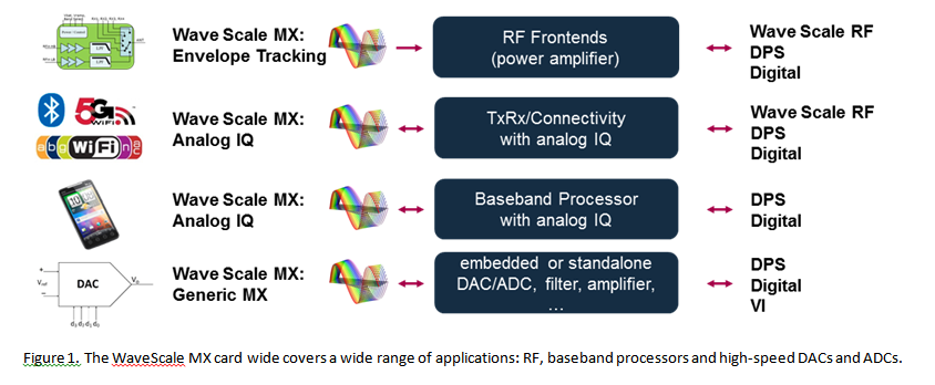
 Advantest participated in the annual SEMICON West show at San Francisco’s Moscone Center from July 12-14, 2016, showcasing a broad spectrum of semiconductor test solutions and highlighting a number of new product introductions. Under the theme, Measure the Connected World … and everything in it, Advantest debuted three new modules for the V93000 single scalable platform. The new
  For customers in the memory IC market, Advantest displayed the high-productivity T5830 memory tester, offering low cost of test for virtually any Flash memory.
 In addition, Advantest showcased other offerings including the company’s