Pages Menu
Categories Menu

Posted in Top Stories

Known-Good-Die Testing of Complex Digital ICs

By Dave Armstrong, Director of Business Development, Advantest America, Inc.

Large, thin and high-power digital ICs pose a number of challenges to the test process necessary for achieving true known-good-die (KGD). As these costly, fragile devices are destined for advanced 2.5D and 3D packaging solutions, advanced test capabilities and solutions must be implemented to reduce scrap assemblies and improve product margins.  Producing a true KGD prior to assembly requires bringing final test and potentially system-level test content forward, executing it at the die level.  This calls for an advanced thermal control (ATC) system, similar to what is traditionally used at final test, as well as fine-pitch probe alignment capability that exceeds the capability of leading-edge wafer probers.  These are the two areas that Advantest aims to address with its die-level handler. To understand the product’s benefits, it’s important to look at the packaging landscape that gave rise to its development.

The assembly and packaging process is changing rapidly, with multi-chip assemblies becoming mainstream.  When multiple devices are assembled together in one assembly (either 2.5D or 3D), the yield risk is driven by the lowest yielding device. Unfortunately, costly, high-yielding memory stacks may need to be scrapped because of undetected faults on other devices in the assembly.

Further complicating this situation is that high- and/or low-temperature testing is often needed to detect many of the marginal faults in a device.   Traditional wafer probers lack a thermal control system responsive to on-die temperature variations.    Other techniques (sticky tape, wafer frames, etc.) lack a viable thermal interface to the device-under-test (DUT), making thermal control very difficult or more likely impossible.

The Advantest HA1000 die-level test system reduces the risks associated with 2.5D and 3D assembly, providing a way to handle, chuck, probe, and thermally control singulated thin die, die stacks, 2.5D assemblies, and even partially assembled 2.5D devices. Features support probing of pads, bumps, pillars, or even through-silicon vias (TSVs) with pitches down to 50 microns or smaller.

Today’s KGD test challenges

The earlier KGD tests can be performed, the lower the test and yield costs, as well as the overall cost of goods sold. Today, both memory and logic performance testing and burn-in are being implemented as early as possible in the device test flow. This KGD testing of multi-die, 2.5 and 3D devices at the die level prevents more costly yield loss later at package-level test, as it identifies process problems earlier so they can be corrected to prevent assembling bad die on otherwise good assemblies. Without this step, yield cost will be higher in 3D chip manufacturing and 2.5D and 3D packaging, as well as for systems-in-package (SIPs) and multi-die devices.

Package-level testing usually runs high-performance tests prior to board and system assembly, driving up power and thermal control requirements. Additionally, package-level burn-in can increase this requirement by 1.5x to 2.5x and drives ATC requirements. As chips and systems become more integrated using 3D packaging technologies, this performance and reliability KGD testing will be required much earlier, at the wafer and die levels, before package assembly.

Pre-assembly die-level and partial-stack test insertion could provide a way to execute high-power thermal tests. The Advantest HA1000’s ATC, together with an extremely low thermal resistance, supports high-power scan tests, elevated voltage screens, dynamic voltage screens and other test techniques to perform die-level sorting prior to stacking. This increases the shipped products’ quality level and screens for new reliability defects that may have been introduced during the thinning, bumping and sawing steps.  Due to the reduced thermal mass, the ATC can also perform single-pass, multi-temperature testing by cycling temperatures several orders of magnitude faster than traditional wafer probe systems.

The value of adding a test step

While it is possible to use this type of prober to replace wafer probe itself, it’s proving more valuable when additional test insertions are made into a traditional manufacturing flow. Adding a pre- or partial-assembly test step requires a financial analysis to confirm its return on investment (ROI). Figure 1 indicates that the return on the test investment is 10 percent or more if the product yield is less than or equal to 93.3 percent (assuming the COT is a conservative 10 percent).

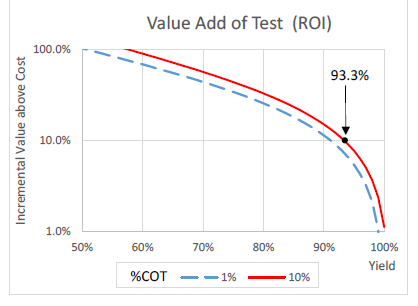
Figure 1: Single Chip = Value of Testing (ROI)


When considering the addition of a new test insertion prior to an assembly step involving the cost of additional chips, the same approach can be utilized to determine ROI.   As shown in Figure 2, if the additional chips (or interposer/package) are 3x the cost of the component being added, the ROI for additional testing prior to assembly is 10 percent or greater if the yield of the last device is less than or equal to 99.6 percent.   Of course, a more realistic back-end yield would provide a significantly higher ROI. 

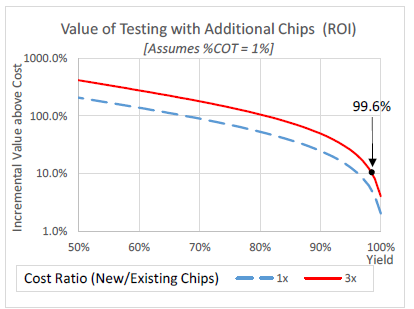
Figure 2: Single Chip = Value of Testing (ROI)

A new approach: singulated die handling and testing

The Advantest HA1000 is a device-level handler for bare die stacks and partially assembled devices. Main features include precise, vision-based alignment; the ability to handle a wide range of device sizes and thicknesses; support for very high-pin-count probing; and integrated high-power-capable active thermal control.  Depending on the size of the device and temperature setpoint, the HA1000 can heat or cool parts of up to 300 watts. The handler incorporates a flexible, dual-fluid thermal control system that can accommodate temperatures in the range of -40°C to +125°C.

A prime advantage of the die-level tester is that it allows devices to be tested after wafer thinning, bumping and dicing. Testing devices in die form detects not only faults from the assembly process (chipping and cracking) but also untested faults, which are typically handled at final test, for more complete KGD test.

Placing and probing thin die

Probably the most critical step for probing raw thinned devices is a world-class vision alignment system capable of positioning the probes appropriately on top of the fine-pitched device structures. For large and high-power thin die, an additional challenge is to apply enough probe force to ensure equal low contact resistance and thermal resistance across the entire die while not damaging the thin die.

The chuck must be carefully balanced to provide good surface area for thermal conduction. The HA1000 does this by using a monitored three-zone vacuum, ensuring that all corners of the die make solid thermal contact to the chuck. If suitable vacuum is not achieved in all three regions, an alarm sounds and the test stops.  The chuck is carefully designed, using micro-channel technology, to avoid hot spots or temperature gradients.   

Conclusion

The Advantest HA1000 provides the industry with a unique opportunity to achieve true known-good devices at the die level – prior to assembly. By carefully positioning thin or thick, large or small devices on a fast-responding thermal chuck, it enables final and/or system-level testing to be conducted earlier in the manufacturing sequence. Performing this extended testing prior to assembly helps ensure that all the parts integrated into a 2.5D or 3D structure are high-yielding, highly reliable devices.  Further, this additional test step reduces scrap assemblies and reduces product cost.  As a result, the ROI for an additional die-level test step is excellent.

For further reading:

Known-Good-Die Test Methods for Large, Thin, High-Power Digital Devices by Dave Armstrong and Gary Maier; International Test Conference, 2016.


More Info:  

Read More

Posted in Featured

Driving a New Paradigm: How the IoT Is Transforming Test


In this issue’s Q&A feature, we talk with Derek Floyd, director of business development for Advantest America. Derek has presented at multiple conferences and workshops on the changes being wrought on the test industry by the advent of the Internet of Things (IoT), and how Advantest is uniquely addressing these challenges.

Q: What is driving technology requirements in today’s tech industry?
A: Over time, the industry has been driven by integration: more and more functionality is being integrated into end products. Mobility has been, and will continue to be, the predominant catalyst. However, in the IoT era, these mobile devices now also serve as infrastructure hubs for peripheral devices from which they obtain information. This is driving increased value. Many capabilities are being accessed via mobile products – with our smartphones, we can now get all our data from the cloud, manage our personal networks, monitor our health and fitness, and control automation and security in our homes, to name just a few applications. This is fueling an increase in silicon volume, along with the massive increase in automation, particularly in the automotive space… all of which is enabled by higher integration.

interview2

Q: Given this backdrop, what are the most prevalent areas in which IoT technology is impacting test?
A: Two key areas are analog integration and power management. In the IoT space, analog functionality and accuracy become more and more important given the volume of analog devices being deployed in mobile products. In turn, power management must be highly efficient to sustain battery life. Batteries need to be used and managed efficiently, so that your smart device can reliably turn off or go into sleep mode when necessary to extend battery life.

Another important aspect is wireless connectively – we need more of it, and we need it more quickly. Carrier aggregation is increasing bandwidth, so wireless connectivity must be able to handle it, as well as more data and applications. Low-power device connectivity is a particular concern for wearables, which are connected into an infrastructure that’s being required to handle very large amounts of data traffic.

Consumerization means lower cost, drives volume – test is close to end of the manufacturing chain, and that creates pressure to lower the overall cost of test and make devices more economical to produce and ship. We need to shorten time to production test and increase the amount of parallelism. When you purchase a test cell, it can cost hundreds of thousands of dollars, so you need to test as many devices as possible per hour to justify the cost. In addition, many peripheral chips are sub-dollar devices, and this further increases the pressure to slash test costs and test times.

Q: What steps has Advantest taken to address these burgeoning IoT test requirements?
A: Quite some time ago, we decided as part of our strategy to focus on a tester-per-pin architecture – all of the functionality is behind every pin. We believe that using this test processor architecture is critical; then all we have to do is change out the front end as needed. We started doing this for digital test first – using a digital card with the same test processor and same memory – then we created device power supply cards, and now we put it into all the analog and RF cards.  The V93000 is a true per-pin architecture, which gives us a lot of flexibility. Our concept is to have as many universal pins on the tester as possible, so we can test almost any type of device, with the highest levels of parallelism.

Q: in what other ways has integration influenced the test process?
A: Integrating anything allows you to make it smaller. Testers historically were very large machines that cost $1 million or more. Now, if you integrate more and more functionality into the cards, you need fewer cards in the system, which means the infrastructure can be very small. Testers for IoT can now cost as little $100,000. This is one of the key benefits of getting the cost out of test – by increasing integration and putting much smaller ATE in place, you can greatly lower your cost of ownership. And if the cost of the part is only cents, you need to test quickly and test many devices – 64 or 128 – in parallel.

Q: How do the Wave Scale cards for the V93000 help advance these objectives?
A: Wave Scale features a high degree of integration. The RF aspect is especially important because everything related to the IoT has some degree of connectivity today, such as smart watches connecting to your smartphone via Bluetooth or some other RF interface. Wave Scale RF has four independent RF subsystems and 32 RF ports per card. With greater integration, we can fit more channels on the board and multiple boards in a system, which means we can increase parallelism, as well as control everything via a sequenced approach – just the same way you’d test everything digitally. Again, our goal is more capability, and more parallel test.

Q: Can you provide an example of how the multi-site parallelism works?
A: If you look at Figure 1, with one board, we can test 16 devices doing transmit (Tx) test and 16 devices doing receive (Rx) test, and then we can just flip them about. We can literally test 32 devices in parallel. This enables us to reduce the overall cost of test of the devices. With this approach, instead of taking 1 second to test a single device, we can test 32 devices in that same 1 second. Thus, combining the Wave Scale card with the V93000 lets you address the three key blocks for IoT: digital, analog and RF.

Q: Aside from consumer and wearable devices, what are key applications where this is essential?
A: For IoT, specifically, you have sensors – the most prevalent use of sensors is in the automotive area. Power management is critical, the microcontroller (MCU) is critical because the application requires very low power and high functionality and is highly integrated, and then there’s the connectivity. The number of sensors in vehicles continues to grow – they’re now in the double digits and moving into the triple digits because sensors are doing everything. Early on, sensors were used for engine management and tire pressure monitoring systems; then, they were implemented for lane control and radar that estimates distance between vehicles for forward collision. Now, we’re also seeing sensors for parking and cameras, measuring individual driver performance, handling acceleration and deceleration, and being used for feedback in the braking system.

Q: How does your approach compare to competitive IoT solutions?
A: Our single platform that can cover everything greatly appeals to customers when they’re comparing us to our largest competitor, which still has several different, disconnected products in its portfolio. So, for example, with the V93000, we can easily scale down in terms of low-cost digital test or to compete in the cost-sensitive analog space, whereas they have a completely different tester for each application. This also allows us to scale up configurations and offer very high levels of integration and high pin counts, which they simply cannot do. We offer a degree of flexibility, scalability and future-readiness with the V93000 that they can’t match. A smaller competitor is trying to match our strategy and go the single-platform route, but they can’t match the integration and level of functionality and performance that we offer.

Another aspect relates to the nature of IoT devices. Because the IoT tends to involve a large number of peripheral devices, they can be miniscule, with very low pin counts, but will still be made in high volumes. Some companies try to get by with using ultra-low-cost tester platforms, but these products tend not to deliver satisfactory throughput or to be able to scale upwards for high parallelism. Because the semiconductor industry is very mature, we have worked hard to demonstrate that you can viably take out much of the cost of test compared to traditional ATE. Over the long term, the V93000 can be used to test virtually anything, and becomes highly cost-effective to have on your test floor.

Q: How do you see the IoT industry evolving over the next five years?
A: I believe that the IoT category, which we define as peripheral devices that deliver data, will explode in terms of unit volume. That’s huge because it is all very low cost. The biggest challenge for test is that many people in the industry will argue that test isn’t really a value-add; it’s a necessity. However, delivering quality to the end customer is essential, so we need to make sure that we can validate all this silicon cost-effectively. This will be a continuous challenge over the next few years: can we test these devices effectively and economically? If you’re spending a lot of money on something as a consumer, you expect a quality product – you can’t have a high-end product breaking because of a 5-cent part. The onus on the industry is to make sure we deliver quality parts to the end customer – it’s essential in automotive, but even for consumerization it’s also vital. If you buy a $100 smart watch, you expect the heart rate monitor to work correctly over the full lifetime of the product.

Quality is important, and the reputation of the company is key. If you want to be a supplier to a major manufacturer, you need to make sure you can guarantee quality. In the past decade, tester cost has gone down by more than half, but throughput per test cell is up by fivefold. The V93000 per-pin architecture has matched this trend, and this is a big advantage for Advantest in being able to continue reducing test costs year over year.


Read More

Posted in Upcoming Events

Advantest Promotes Newest Test Solutions at Technical Kiosks During Semicon Taiwan


Advantest marked the occasion of Semicon Taiwan to host a two-day hospitality event at which customers were invited to learn about the company’s new products and solutions while networking and enjoying refreshments in a relaxed setting.   With solid attendance on both days, this year’s event recorded the highest level of participation of the event’s five-year history.

Product kiosks within the suite included those focused on:

-Smart Testing of Smart Devices

V93000 AVI64 Universal Analog Pin

avi64-st

-Delivering Revolutionary Test Capabilities for the Next Wave

NEW V93000 Wave Scale Solution

wavescale

-Testing Memory Devices and SSD UFS

T5800, T5830 and T5851 Testers

-Fully-Integrated Digital IC Test Solution

EVA100 Tester

eva100

-Test Floor Intelligence Solutions

Field Service Capabilities

-High Resolution TDR for Failure Analysis

TS9000 TDR option utilizing terahertz technology

ts9000


Read More

Posted in Upcoming Events

Advantest Explores the Internet of Things at SEMICON Japan

semi-west

At the upcoming SEMICON Japan trade show in Tokyo on December 14-16, Advantest will bring the concept of Internet of Things (IoT) directly into our exhibit.  The value of our products and what we enable will be the platform for how the products will be shown in the booth.  Our products and services will be sorted into these four IoT segments: Industrial, Connected Home, Wireless/Wearables, and Connected Automobile.  In addition to over 18 products and services featured in the booth, we plan to have more hardware and live demonstrations for each of these products than in previous shows.

Further, we are utilizing more cutting-edge technology to demonstrate our products including an interactive wall that catches the visitor’s motion, transparent glass LED monitors to display product messages, and the use of augmented reality on Apple iPads to creatively display product information.

In addition, as a Gold sponsor of the show we are sponsoring the Autonomous & Connected Car Forum, where Shin Kimura, vice president of the ASD Test and Measurement Business Group, will present Thursday afternoon.

 Learn more about SEMI Japan.

Read More

Posted in Upcoming Events

Advantest Plays Key Role in ITC with Extensive Program Participation and Exhibition

itc

At the November 15-17 International Test Conference in Fort Worth, Texas, Advantest will demonstrate both hardware and online test solutions as well as serve on panels and present several papers in ITC’s renowned technical program.

In addition to being a Platinum-level corporate supporter of ITC, Advantest also is a Gold-level sponsor of the IEEE Automotive Reliability and Test Workshop, in conjunction with ITC TestWeek™.On The Exhibit Floor

Advantest will feature demonstrations of its on-demand CloudTesting™ Service and its new EVA100 analog/mixed- signal IC test solution.

The first-of-its-kind CloudTesting Service allows users to access various IP selections whenever needed from Advantest’s web site.  Using this on-demand online service, designers can verify their new silicon at very low cost with no capital investment, set up their own test environment within a few hours and be ready to test when the device arrives from the fab.  At ITC, visitors to the booth can see the desktop test station with a live demonstration of how fast a device can be verified with STIL-generated DFT patterns.  With free tester leasing and moderate repair costs, Advantest’s CloudTesting Service allows customers to avoid and unplanned expenses.

Advantest’s new EVA100 analog/mixed-signal test solution combines a modular architecture with high-voltage and high-precision analog parametric measurement units, providing the flexibility to conduct various measurements over a broad range of analog and mixed-signal devices.  The latest model in the EVA100 product family includes an integrated servo-loop function that delivers the industry’s fastest test time and high precision.  Its 18-bit AD-converter characterization has 20bit linearity DC performance and ultra-low drift/noise source and VREF.  Coupled with a GUI that is highly intuitive, users are able to minimize the time to market for their newest ICs.

Technical Program Participation

In addition to product exhibits, Advantest’s technologists will present several papers within ITC’s revered technical program throughout the three-day conference.  Following is a look at where Advantest’s experts will be heard:

  • Dave Armstrong will host a discussion of Advantest’s new HA1000 die-level handler, a cost-efficient test solution for determining known good die (KGD) prior to IC packaging.
  • Bob Bartlett will chair Session 5, a special session on “mmWave ATE HVM Technology,” where Roger McAleenan will present on mmWaveATE challenges.
  • Dave Armstrong will chair Session 6, a special session on “Heterogeneous Integration Pushing the Test Roadmap,” as well as present a paper in that session titled “Moore’s Law is Done and Heterogeneous Integration is Taking Off.”
  • A.T. Sivaram will present a poster co-authored with Xilinx Corporation on “CloudTesting™ Service in Silicon Diagnostics,” which describes an innovative service-oriented test solution for debugging high-end FPGA devices.
  • Neils Poulsen along with Alfred Crouch and Jim Johnson of SiliconAid will present a poster titled “Silicon Debug on ATE Using Protocol-Aware JTAG-IJTAG EDA Software Tools.”
  • Dave Armstrong along with Gary Maier of IBM will deliver a paper on “Known-Good-Die Test Methods for Large, Thin, High-Power Digital Devices.”
  • M. Ishida and T. Kusaka of Advantest along with T. Nakura, N. Terao, R. Ikeno, T. Iizuka and K. Asada of the University of Tokyo will present a paper titled, “Power Supply Impedance Emulation to Eliminate Overkills and Underkills Due to the Impedance Difference Between ATE and Customer Board.”
  • T. Nakamura and K. Asami’s paper “Novel Crosstalk Evaluation Method for High-Density Signal Traces Using Clock Waveform Conversion Technique” will also be given.

The four panels held during ITC TestWeek™ will each feature panelists from Advantest.  Dave Armstrong will serve on Panel 1, “The Unknown Unknowns of Test,” while Roger McAleenan will participate on Panel 2, “Phased Array 5G:  Is Test Connected or Disconnected?”  Bob Bartlett will bring his expertise to Panel 3, on test cost reduction, and Holger Engelhard will participate in Panel 4, which looks at ATE today, and where we should be heading.

More information about ITC.

Read More