Pages Menu
Categories Menu

Posted in Featured Products

New Pick-and-Place IC Handler Improves Efficiency in High-Volume Semiconductor Manufacturing and Device Characterization

With an eye on helping customers keep pace with the rapidly evolving system-on-chip (SoC) market, Advantest’s new M4872 pick-and-place handler is designed to rapidly adapt to changes in device technology.  It offers improved productivity in testing SoC devices in high-volume manufacturing (HVM) and device characterization pre-production environments. 

The new handler matches all of the leading-edge performance specifications of its predecessor, the M4871, including throughput of up to 15,000 units per hour, in a footprint that is approximately 10 percent smaller. The portable M4872 handler has advanced vision-alignment capabilities and can accommodate an optional active thermal control system.

The vision alignment-equipped M4872 incorporates a common change kit, which saves time and money and also significantly shortens time to market.  In total, the time it takes to change device types is reduced by more than 45 percent, enabling nearly twice the throughput of handlers that rely on standard change kits.

Advantest’s proprietary on-the-fly vision-alignment technology precisely positions devices under test, making the new handler ideally suited for testing fine-pitch ICs and devices with both top- and bottom-side contacts. The resulting improvements in test yields and cycle times contribute to higher overall productivity.

The M4872 also includes an automatic re-test function that transfers all failed ICs into the loader stocker, helping to avoid time-consuming operator assistance and reducing IoT test times by 20 percent or more.

The scalable M4872 handler is compatible with the V93000 platform for low-cost testing in R&D and high-mix, low-volume production.  Handler operation is made simple by a user-friendly GUI with pre-defined functions.

Find out more:

Read More

Posted in Upcoming Events

SEMICON JAPAN 2016 – Advantest Ushers in a New Era of IoT Solutions

Advantest showcased an innovative booth in celebration of SEMICON Japan’s 40th anniversary during SEMICON Japan, held December 14-16, 2016.  Inspired by the Internet of Things (IoT) theme, Advantest’s booth was divided into the four segments of IoT:  Connected Homes, Connected Automobiles, Industrial, and Wireless.  Showcasing 19 of its products and services, the displays included several interactive demonstrations that incorporated virtual reality and augmented reality techniques, as well as mock-up system displays. The interactivity of the booth attracted quite a lot of attention from visitors including customers, partners and media.

In addition, Advantest received two awards at the SEMI President’s reception.  The first was presented to former President and CEO Shinichiro Kuroe for his many years of support and participation at SEMICON Japan, and the second award was presented to Chairman Toshio Maruyama for his significant contributions to the fields of sales and marketing throughout his career in the semiconductor industry.   

Advantest also participated in the technical program with a presentation in the Connected Automobile area delivered by Shin’ichi Kimura, Vice President, ASD Test Business Group. Overall, SEMICON Japan 2016 drew over 64,000 attendees.

Opening day of SEMICON Japan 2016

The booth featured 19 products and services

Read More

Posted in Upcoming Events

Advantest Opens Registration for the VOICE 2017 Developer Conference with the Theme of “Measure the Connected World and Everything in It”

Advantest opened registration to attend its VOICE 2017 Developer Conference being held in Palm Springs, California, on May 16-17 and Shanghai, China, on May 26. As VOICE kicks off its second decade, both conferences will feature the theme “Measure the Connected World and Everything in It.”

This theme is a guiding principle that reflects Advantest’s company-wide commitment to test, measure, analyze and report on the most critical performance parameters of the smart semiconductor devices that enable the ever-expanding Internet of Things (IoT). Advantest’s technologies touch all ICs that enable today’s interconnected world, helping to improve the ways people communicate, conduct business, access entertainment, manage life, and more.

At VOICE 2017, attendees will have access to wide-ranging learning and networking opportunities, including general sessions, social events and technical presentations focused on eight topic areas (hot topics, device-specific testing, hardware design and integration, improving throughput, reducing time-to-market, new hardware/software test solutions, test methodologies, and product engineering). Additionally, the conference will showcase its sponsor partners in a special Expo area, and the VOICE Technology Kiosk Showcase will expand to include more interactive discussion sessions in both locations.

The general session in Palm Springs will feature a keynote on Cyber Security by former FBI special agent Chris Tarbell, one of the most successful cyber security law enforcement officials of all time. More program information is available on the VOICE website at https://voice.advantest.com.

Attending VOICE 2017

Online registration is now open at https://voice.advantest.com/register. The 20-percent early bird registration discount for the Palm Springs event ends March 10. Those interested in attending the VOICE China event should email mktgcomms@advantest.com for more information. The presentations in China will be in Mandarin Chinese.

Registered VOICE 2017 attendees are encouraged to make their hotel reservations early. The deadline for the Hyatt Regency Indian Wells Resort & Spa in Palm Springs is April 14, 2017. Additional hotel information for both venues is available on the VOICE website at https://voice.advantest.com/hotel-reservations.

Visit VOICE 2017


Read More

Posted in Top Stories

Enabling High-Volume Optical and Electrical Test on 100Gbps Optical Interconnect Devices

By Tasuku Fujibe, Consulting Manager, and Hiroyuki Mineo, Senior Engineer, Advantest

High-speed data communications demand is rising at astronomical rates. According to a forecast from Cisco Systems, the volume of global data center traffic is expected to increase to more than 10 zettabytes per year in 2019. In response, new network architectures are being considered, while data centers are being housed in much larger buildings. As this requires interconnection devices (switches, routers, etc.) to support distances of as much as several kilometers, using electrical interconnection devices in these very large data centers is becoming impractical. Moving forward, optical interconnection devices will need to be implemented in high volumes, creating new test challenges. Currently, rack-and-stack solutions are used to test these devices, but new manufacturing approaches are needed to avoid the bottlenecks such approaches can create.

To answer this demand, Advantest has developed a test solution with the ability to cover high-speed interconnection devices, both electrical and optical – particularly those destined for high-speed datacom applications. Designed for high-volume manufacturing, the T2000 scalable test platform can be configured to test current digital signal processors (DSPs) as well as high-speed buses and communication interfaces due to its modular architecture.

Platform offers high flexibility

The T2000 ATE solution consists of a high-speed optical/electrical test module, a low-speed digital module for I2C ports, and a device power supply module (Figure 1), all of which are integrated into the test platform. The test module’s 64 ports can operate up to 28 Gigabits per second (Gbps). This includes 32 optical ports – 16 transmit (TX) and 16 receive (RX) – and 32 differential electrical ports (16 TX and 16 RX). The T2000 platform also includes high-performance device fixture technology for both the optical and electrical ports to perform device interface.

To understand the benefits the T2000 platform enables, let’s take a closer look at the device fixture and the high speed optical/electrical test module.

Device fixture and test module

The device fixture provides both optical and electrical signal connections between the device-under-test (DUT) and the test module. To test optical lanes, the device fixture must support such optical assemblies as MT-connectors. However, ordinary MT-connectors have a limited insertion lifetime (typically, less than 300 insertions), making them inappropriate for this application. To overcome this limitation, Advantest has developed a high-volume-capable non-contacting optical connector that is fully compatible with MT-connectors.

Figure 2 shows the new optical connector and illustrates the approach used for its fabrication. Using a gradient-index (GRIN) lens to maintain a working distance of 150 microns (µm) enabled development of a high-performance optical connection with no physical contact between the end of the fiber-optic cable and the connector.  Because the new connector is MT-connector-compatible, it can be used to make contact with MPO connectors, which are typically used in compact QSFP+ PSM4 transceivers used for data communications.

The high-speed optical port block diagram is shown in Figure 3. FUNC ASIC has pattern generator (PG) and bit error rate tester (BERT) functionalities, both of which can operate up to 28 Gbps. For electrical ports, the FUNC ASIC is connected to the DUT via the device fixture. For optical ports, the output test signal from FUNC ASIC goes to the optical modulator to modulate the continuous wave laser provided by the laser source. Variable optical attenuators (VOAs) adjust output power to the DUT to test the DUT’s receiver sensitivity. The optical signal provided to the DUT is connected to a photo detector and trans-impedance amplifier (TIA) in the test module to convert it to an electrical 28-Gbps signal. Then FUNC ASIC captures the signal to measure eye diagram by using its BERT capability.

Measurement results

During device fixture evaluation, insertion loss variation was measured against iterations. The results, seen in Figure 4, showed stable insertion loss variation of less than +/-0.3 dB during 100,000 repeated operations. Compared to ordinary MT-connectors, which have an anticipated lifetime of less than 300 cycles, this connector can provide stable measurement with a longer lifecycle.

Current 100-Gbps datacom transceiver interfaces, such as PSM4, CLR4 or CWDM4, use four lanes of both optical and electrical 25-Gbps lanes to achieve aggregated band width of 100-Gbps. The test module has 16 lanes of both optical and electrical high speed ports. The scalable platform can simultaneously test four DUTs per optical port module; integrating two modules onto a test solution thus allows parallel test of up to eight DUTs. Multi-site testing increases system throughput and significantly drops per-site equipment costs.

Summary

The semiconductor industry roadmap for optical transceivers – advanced semiconductor devices that transmit and receive data through optical fibers – calls for boosting speeds from today’s 40-Gbps interconnections to as much as 400-Gbps by 2020. Advantest’s T2000 solution is among the first integrated solutions able to cost-efficiently test these high-speed devices.

Since typical 100G transceivers use four 25-Gbps ports to achieve aggregated bandwidth of 100-Gbps, the T2000 configuration allows four 100-Gbps devices to be tested simultaneously, improving test throughput and reducing system cost. It also includes a device fixture solution that provides stable and longer-lifecycle non-contacting optical connectors, making the system well suited for high-volume manufacturing environments.

Find out more:

Read More

Posted in Top Stories

IoT Devices Require a New DFT Paradigm and Scalable ATE

By Neils Poulsen, Director of SoC Business Development, Advantest

Touted as the “next big thing” to drive the next major wave of semiconductor device growth, the emerging market for the Internet of Things (IoT) is widely projected to increase semiconductor device volumes by tens of billions of units over the next several years. These volumes will be fueled by myriad new consumer end-user applications and services, to be provided by hundreds of companies ranging widely in size and resources.

IoT devices comprise several functions: computation (typically a microcontroller); communication (typically a wireless/radio frequency [RF] connection); and multiple sensors and/or actuators, the quantity of which depends on the end-use application. Sensors are used to detect environmental parameters, such as temperature, acceleration, magnetic field, moisture, light intensity or distance. The received signals are processed via integrated microcontroller or DSP cores, and the information is passed on to wireless devices via wireless communication interfaces. The integrated cores’ performance is significant, as data encryption is often required due to security aspects in IoT products. Other key functional components in smart devices are drivers for actuators to convert electrical signals into movements. Typically, these are integrated driver circuits for brushless DC motors or relay drivers.

Because these devices must operate on small batteries for extended periods of time – sometimes years – they must be able to consume very low amounts of power. Bluetooth Low Energy, ZigBee, WiFi and other communications standards are designed for low power requirements and optimized for easy network integration. This combination of requirements presents many challenges to designers and test engineers, as these complex devices are increasingly becoming more like high-end systems-on-chip (SoCs), but necessarily sell at a small fraction of the price.   

Moreover, the dynamic nature of the consumer market, as well as the large number of competing companies, is placing tremendous pressure on semiconductor suppliers to shorten both their time to market (TTM) and time to quality (TTQ). Improving these parameters will allow them to secure customer design wins and achieve the necessary volumes and quality levels their customers require – at the same time, meeting their own cost targets, including acceptable manufacturing yields (see Figure 1).
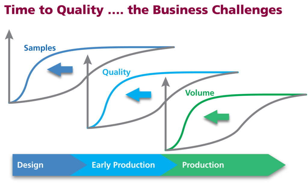
Figure 1

To profitably compete in the IoT market, companies must find ways to significantly increase their overall efficiency and reduce their overall costs. This means they must consider breaking away from their traditional approaches and embrace a new paradigm for the design-to-manufacturing process, including test.

Changing the paradigm

In the traditional process flow (Figure 2), design and DFT (design-for-test) engineers use test instrumentation in benchtop setups during initial device bring-up to debug and verify the chip’s proper operation. This includes building special fixturing to interface the device-under-test (DUT) to various multiple instruments, as well as translating patterns from the design simulation environment into test vectors that can execute in the benchtop instruments to control and stimulate the DUT. To test complex IoT chips’ complete functionality (i.e., digital, analog and RF) as they become more integrated, these engineers typically write time-consuming custom software routines to control and coordinate multiple benchtop instruments.
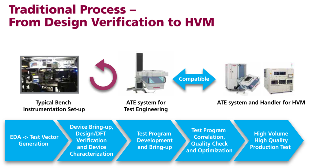
Figure 2

Similarly, in the next step of the traditional process, the characterization phase, engineers typically use benchtop instrumentation to evaluate the chip’s performance, validate specifications, and determine operating margins across a range of operating conditions, including frequency, voltage and current. This can be a time-consuming, manual process. In addition, the instrumentation, device fixturing and custom software routines usually differ from those used in the design verification phase. This leads to inefficient duplication of engineering resources and can create delays in the overall process.

To garner a statistically valid sample, many devices should be characterized, but collecting and analyzing the large amount of data needed to do this is limited by the slow throughput and difficulty of interfacing bench setups to automated device handlers. As a result, because of TTM pressures, only a few devices usually receive this high level of characterization, and the range of operating conditions is limited, which can negatively impact quality and device yields later during the manufacturing process. This is also typically the phase when customer samples are first provided, based on characterization data, so time-consuming benchtop characterization limits the number of sample devices that can be shipped to customers, which can limit market potential.    

In the next phase of the traditional process, test engineers develop test programs on ATE that will be used to test the devices in high-volume manufacturing (HVM). However, the ATE instrumentation, DUT fixturing and software environment are all very different than the bench set-ups. This means there is very little compatibility between the earlier Design Verification and Characterization phases and the HVM Test Program Development phase. Once again, this results in duplication of engineering effort, including designing new DUT interface fixturing, performing additional ATE characterization to correlate to the benchtop characterization data, and determining test limit guard-bands to ensure HVM test quality. The different environments also mean that correlating the HVM test results to the benchtop data can be difficult and time consuming, requiring multiple iterations and further delaying TTQ.

Implementing a new approach

A new integrated ATE solution being embraced by several leading semiconductor suppliers utilizes engineering ATE that comprises the same hardware instrumentation, software environment and DUT interface fixturing as the ATE used for HVM test (Figure 3).  This compatibility accelerates test program development and bring-up, correlation and release to HVM by leveraging the engineering efforts from the previous phases – resulting in reduced costs and improved TTQ.
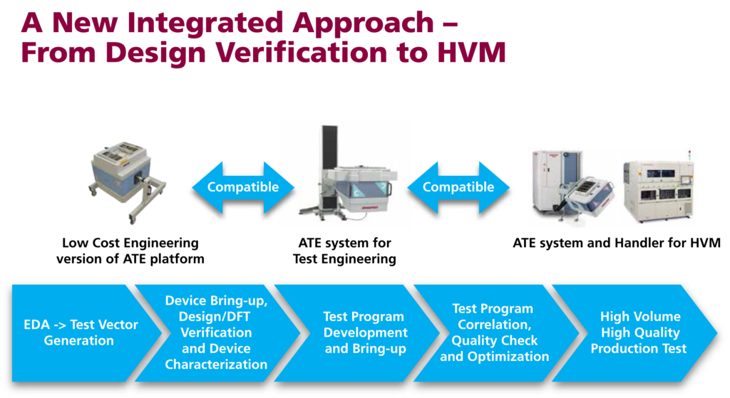
Figure 3

Design/DFT engineers can utilize low-cost engineering ATE for their initial device debug and verification so that when they translate their simulation patterns to test vectors, these same vectors can be used by test engineers for their HVM test program. This eliminates redundant vector translation, enables test engineers to begin test program development earlier, and minimizes problems and delays due to revision errors.

Similarly, by combining low-cost ATE with a cost-effective engineering handler, an automated “production-like” environment and high-throughput characterization test programs, engineers can realistically characterize thousands of engineering samples in far less time, significantly reducing TTM. And by collecting and analyzing much more data over a far wider spectrum of operating conditions, they can significantly increase quality.

Advantest V93000 platform handles multiple requirements

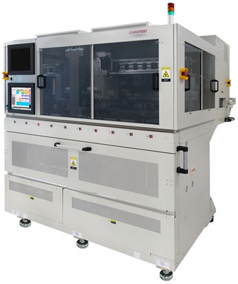
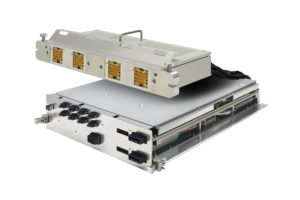
Advantest is enabling this integrated test approach via its V93000 platform of testers, which includes the scalable A-Class configuration. A cost-effective engineering ATE solution, the A-Class uses the same hardware instrumentation, software and DUT interface fixturing as the other members of the V93000 family (see Figure 4), facilitating transition across the V93000 platform as needed. This includes high-density instruments that utilize the universal pin concept (every pin can generate and receive the digital, analog or RF signals needed to test IoT devices).
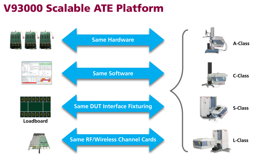
Figure 4

Utilizing the V93000 A-Class in engineering for design verification and characterization creates a seamless streamlined process, in which:

  • Performing the initial device debug and bring-up on the same DUT fixturing that will be used in HVM enables removing the loadboard from the critical path;
  • Reusing common test routines speeds up the entire DV-to-HVM process and can result in having the HVM test program complete with first customer samples; and
  • Automated high throughput characterization (in conjunction with an engineering handler) provides faster and higher-volume data collection, on a significantly larger number of devices.

Implementing the Wave Scale RF channel card makes the V93000 A-Class even more effective as an economical engineering option for the IoT market. Wave Scale RF was designed with four independent subsystems per board to eliminate shared pin resources. This enables both in-site and high multi-site parallel testing, helping achieve test time reductions of up to 50 percent or more, compared to traditional RF architectures.

Through the combination of all these capabilities that allow users to conduct their engineering activities on the same platform and instrumentation set that they use for high-volume production, Advantest has developed a scalable solution that improves engineering efficiency, lowers overall costs, reduces TTM and improves TTQ – helping semiconductor suppliers to compete in the emerging IoT market.

Find out more:

Read More