Pages Menu
Categories Menu

Posted in Upcoming Events

VOICE 2017 Set to Kick Off this Month in Palm Springs and Shanghai – Technical Program Details Now Available for Both Venues

VOICE, the annual developer conference hosted by Advantest Corporation, will kick off its second decade on May 16-17 at the Hyatt Regency Indian Wells Resort & Spa in Palm Springs, Calif. The conference will again be held in dual locations, with the U.S. event being followed by VOICE China on May 26, at the Intercontinental Shanghai Pudong in Shanghai.

With a record number of technical presentations, an expanded Technology Kiosk Showcase, and a new technology track, this year’s program is shaping up to be the most exciting yet. The dual-venue VOICE 2017 agenda includes three diverse keynote speakers, a Partners’ Expo, and interactive discussion sessions for users of the V93000 and T2000 system-on-chip (SoC) test platforms, as well as Advantest test cell solutions.

This year’s technical program features a roster of papers from Advantest’s worldwide customers, partners and employees, all presenting insights and best practices. Technical topics will cover device-specific testing, hardware design and integration, improving throughput, reducing time-to-market, new hardware/software test solutions, test methodologies, product engineering, hot topics in the ATE industry, and — for the first time – SmarTEST 8.0 for the V93000 platform. At both events, additional topics will be spotlighted in technical kiosks staffed by Advantest R&D, industry experts and technologists. The kiosks at VOICE China are expected to reach record numbers this year.

In addition to the rich technical content, VOICE 2017 features exciting keynote speeches each morning. The Palm Springs event will get underway with a talk by Advantest’s own Hans-Juergen Wagner, senior vice president of the SoC product group. His presentation, “The Future Trends for and Contributions of Test in the SoC Market,” will detail the drivers, challenges and emerging trends of SoC device designs and their impact on test. The second day’s keynote speaker will be former Federal Bureau of Investigation (FBI) special agent Chris Tarbell, one of the Bureau’s most successful cyber security law enforcement officials of all time. His must-attend presentation sheds light on information too sensitive for print. In Shanghai, Dr. Peter Chen, senior director of China business development at TSMC China Company Limited, will share his insights into the global semiconductor industry landscape, technology trends, and especially the ecosystem and market in China.

Opportunities for face-to-face interaction will be available at various networking activities, including a don’t-miss evening event in the Enchanted Desert near the San Andreas Fault Line in Palm Springs. In addition, a Partners’ Expo will be held in both Palm Springs and China for sponsors to showcase their advanced solutions related to semiconductor testing.

To register for the U.S. event, go to https://voice.advantest.com/register. Online registration closes May 11. On-site registration is available at an increased fee.

Those interested in attending the VOICE China event should email mktgcomms@advantest.com for more information. The presentations in China will be in Mandarin Chinese.

Follow us at #VOICE2017 on Twitter @Advantest_ATE


Read More

Posted in Top Stories

RF Test Requirements Driven by Emergent Package Integration

By Judy Davies, VP, Global Marketing Communications, Advantest Corp.

The many connected tasks we perform every day using advanced mobile products, such as smartphones, tablets and notebooks, are enabled by a somewhat dizzying array of wireless standards. These range from Long Term Evolution (LTE), LTE-Advanced, LTE-A Pro and LTE-M smartphone standards, to ZigBee, Bluetooth, GPS and Wireless Local Area Network (WLAN). The requirements and performance criteria for these wireless technologies differ according to their application – many of which revolve around the Internet of Things (IoT) – creating a host of technological challenges, including those surrounding packaging and test.

Before they’re packaged, assembled and shipped, RF-based system-on-chip (SoC) devices built on the current Third-Generation (3G) and Fourth-Generation (4G) LTE broadband standards are fully tested and characterized, as are both the RF and analog baseband transceivers employed in these applications. In addition, the Fifth-Generation (5G) standard is forthcoming, with its promise of new speed and capacity levels, lower latency and greater flexibility than LTE, but its new encoding technologies and chip structures will require new production, packaging and test technologies. The anticipated needs of next-generation wireless networks are in fact shaping the next generation of RF test equipment.

The proliferation of advanced packaging methodologies – e.g., fan-out wafer-level packaging (FOWLP), multichip packages (MCPs), through-silicon vias (TSVs), embedded passives and actives, and systems-in-package (SIPs) – also plays a key role in growing RF test requirements. While it’s not clear which of these package types will dominate going forward, they are all impacting how steps such as wafer sort, final test, packaging test, burn-in and others are performed.

Packaging integration is key

With respect to packaging for RF transceivers, as well as for RF chips in general, every RF device comprises a large number of passive components, such as capacitors and inductors, allowing its use as an end product. Therefore, packaging integration is essential to turning RF silicon into a device that can easily communicate with the antenna in the RF space. The three primary components of integrated packages are as follows:

  1. Embedded passive devices – embedded passives are essential to making useful RF end products based on RF chips, and they are a key value-add provided by outsourced semiconductor and test (OSAT) houses.
  2. Multiple standards – many standards are integrated into today’s mobile phone, so it’s critical to implement an RF set that can handle these various standards. Multi-purpose RF devices switch modes when the user switches location, which makes them more both complex and more challenging to test.
  3. Multiple antennas – essential to ensuring that a device will work no matter how it is held by the user, multiple antennas are increasingly being employed within wireless products.

OSATs are competing with each other to unify all of these components into a viable RF package. Flexible, scalable automated test equipment (ATE) is a fundamental requirement for thorough testing of these devices. This includes both early die sort and final test once the peripherals and passives are attached within the integrated package. Regardless of the packaging technique, more rigorous functional test and more robust compliance test are essential – highlighting the importance of precision, capability and bandwidth in new equipment. Combining a tester-per-pin architecture – such as the Advantest V93000 platform – with massive parallelism is one approach to ensuring the high performance and high utilization chipmakers need to get their products to market more quickly, and at a lower test cost.

Lessons of evolution

Much discussion is under way with respect to how packaging impacts the way test cards are developed – similar to what happened with printed circuit boards (PCBs) a decade or so ago. Back then, board test was big business. Virtually every electronics company created its own PCBs, using its own components, and put them into widely available electronic products. Since then, the PCB chain has consolidated, with a small number of very large subcontract manufacturers putting out PCB assemblies.

Package integration also faces a similar major change – more and more technology is being integrated into a single piece of silicon. PCBs are becoming smaller and smaller, or being eliminated entirely, as in products like the Apple Watch. As this industry shift continues to evolve, the line between chip and package is blurring – particularly with more intelligence being put into the package (which was once merely a “dumb” housing for the circuitry). Competition for business between PCB load and assembly houses and OSATs is also on the rise. What will be chosen depends on whether the customer needs one-stop shopping, which OSATs claim they can provide, or if they’d prefer to tap more traditional PCB load/assembly providers for the board.

A clear winner in this space is chip-scale packaging—particularly, wafer-level chip scale packaging (WLP). The majority of the building blocks in today’s smartphones are WLPs. Eliminating the classic substrate and consolidating the flow of material into wafer-level scale allows two goals to be addressed in one step: miniaturization (making the package ultra-thin) and cost scaling—a key requirement for high-volume manufacturing.

Reducing costs through parallelism

Signal transmission and reception in 5G systems will also impact future test equipment requirements, which are further complicated by the projected billions of IoT devices with different types of sensors using low-power wireless links to connect to the internet. These sensors will be located all around us, letting us access, interact with and control our environment no matter where we are – at home, at work or in transit.

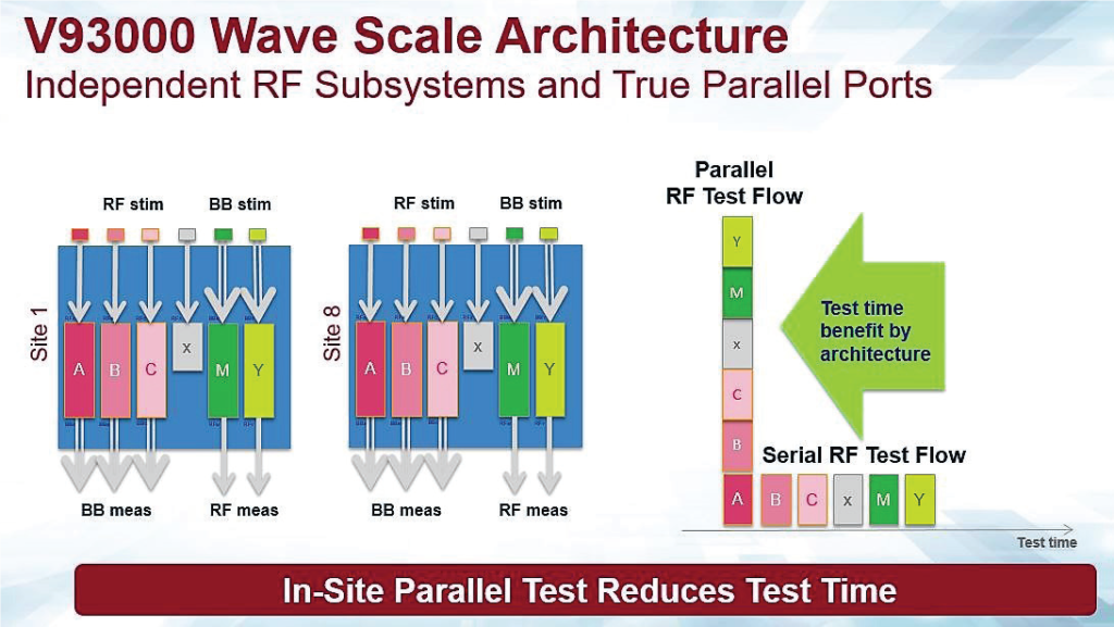
Current RF testing solutions, which typically require multiple cards and a separate calibration kit, employ a fan-out architecture with shared subsystem resources. This means that devices with multiple frequency paths are actually tested in serial within the device, rather than in true parallel test mode. It also means that only one RF standard at a time can be tested per site.

One new approach is Advantest’s V93000 channel card called Wave Scale RF that omits shared resources, condensing four independent RF subsystems into one integrated card with a high degree of parallelism – up to 192 ports for parallel testing of multiple RF device types. This removes the limitations placed on test speedup, cutting test times in half, and enabling device parallelism of 16, 32 or even higher. These cards, together with the complementary Wave Scale MX (for mixed-signal) cards, can simultaneously test multiple standards or multiple paths within each RF device, achieving both in-site parallelism and high multi-site efficiency. Devices can be tested two to three times faster than with other solutions – greatly reducing the cost of test. This is a key requirement for OEMs and fabless semiconductor companies that need to quickly bring RF-enabled devices to market in high volumes.

Wave Scale MX is optimized for analog IQ baseband applications and testing of high-speed DACs and ADCs. As with Wave Scale RF, it omits shared resources, delivering parallel, independent operation of all 32 instruments controlled by a hardware sequencer. This is critical for semiconductor and telecommunications chip leaders, who face a 10x reduction from what they sell into cell phones to what they can charge in the industrial area. From a security perspective, the key challenge is that the functionality must ensure safety, while data is directed into the right channel and properly authorized – thus, the security requirement is even higher than for phone line communication.

In fact, security is one of the biggest concerns about the IoT– silicon providers will be under tremendous pressures to guarantee that their products adhere to industry reference standards. Whether these standards will be as stringent as those adopted within the automotive and aerospace industries remains to be seen, but they will most certainly need to be stronger than consumer-grade standards.

These requirements further underscore the need to rigorously and robustly qualify and test devices, as well as manufacturers’ need to ensure long-term device reliability (based on user demand). This means that the pressure to deliver high-quality devices at the lowest possible investment cost will continue to mount, requiring methodology breakthrough and further justifying the need for advanced equipment that can fully leverage these changes in the RF device landscape. With the new Wave Scale card, OEMs can address their bottom-line manufacturing and test cost pressures while ensuring a solution is in place with the flexibility and headroom to accommodate the requirements of the future.

Read More

Posted in Top Stories

System-Level Test Essential for Fast-Growing Embedded NAND Market

By Ken Hanh Duc Lai, Marketing Director, Advantest America

The market for NAND flash memories is growing at a rapid pace, driven in large part by the massive demand for solid state drives (SSDs), which have replaced hard disk drives for many applications. According to Gartner, the SSD market will reach above 370 million units in 2020, and IC Insights forecasts that memory IC products will show the strongest growth rate through 2021 of the four major IC product categories (the others being logic, analog and microcomponents).

A significant portion of the SSD market is commanded by PC servers and clients used for big data storage applications. However, the mobile market comprising portable wireless devices like smartphones and tablet PCs is growing as well, with variations in form factor increasing to meet new market demands. Driven by these applications, mobile memory unit shipments are forecast to exceed 2 billion units by 2020. These include embedded multimedia cards (eMMC), embedded multi-chip packages (eMCP), MCP and raw NAND. In concert with this growth, the embedded NAND market is undergoing a shift in protocol usage. Embedded NAND is in 80 percent of the smartphones currently on the market, and while smartphones and tablets have typically used eMMCs to store information, a transition is under way from eMMC to Universal Flash Storage (UFS) as the future of flash memory (see Figure 1).


Figure 1. UFS has taken hold, and is expected to represent half the market for NAND flash SSDs by 2020. (Source: IHS Mobile and Embedded Memory Market Tracker Q4 2016)

The JEDEC-defined UFS mobile-centric storage standard addresses next-generation mobile performance and scalability, offering fast sequential read/write speeds with high random IOPS1, which are essential for mobile phones. (For SSDs, random IOPS numbers are primarily dependent upon the storage device’s internal controller and memory interface speeds.) One key value of UFS is its ability to leverage the strengths of several existing technologies in one standard: the low power consumption of eMMC; the MIPI interface standard, M-PHY and UniPro, for the interconnect layer; and the SCSI command set as the application protocol.

Devices based on UFS 2.0, the current version of the standard, offer the highest available performance of any SSD interface standard due to its separately dedicated read/write paths, which enable UFS to read and write simultaneously. At up to 1200 Megabytes per second (MB/s), UFS operates at twice the rate of Serial ATA (SATA) 3.0 and three times that of eMMC5.0. UFS also consumes less total power by processing tasks sooner and staying in standby mode longer. Figure 2 summarizes the key benefits of UFS standard.

Figure 2. UFS offers a number of benefits that make it a superior option for embedded storage in mobile devices. (Source: Universal Flash Storage Association)

UFS is here

Adoption of UFS in the U.S. has already begun, with most of the top 10 mobile handset OEMs using UFS memory for their flagship models. While this includes primarily high-end handsets at the moment, as the cost to implement UFS continues to decline, more and more mid-tier phones will incorporate UFS-based embedded NAND memory devices. Moreover, the ecosystem for UFS is already in place, with a range of vendors supporting the UFS interface, including makers of NAND flash, systems-on-chip (SoCs), operating systems, measurement tools, and testers optimized for high-volume manufacturing (HVM).

Major NAND makers and manufacturers of UFS and BGA2 SSDs have adopted system-level test (SLT) for production use. More than 50 testers overall have been installed since the second half of 2016 for system-level testing of UFS and BGA SSDs, and this number is expected to triple during 2017.

Flexible tester optimized for embedded NAND

Memory IC makers need a class of tester that specializes in SLT of these devices, while maintaining the reliability, low cost and high volume capabilities required for conventional memory testers. Advantest developed its T5851 system-level test (SLT) solution – part of the T5800 platform series – specifically to meet these needs, delivering cost-effective testing of UFS and BGA SSDs. Built with the same proven test architecture used in Advantest’s MPT3000 family of SSD protocol test solutions, the T5851 allows customers to minimize both their capital investments and deployment risks by using the same platform and FutureSuite™ software as other members of the T5800 product line.

The flexible T5851 tester is available in both production and engineering models, allowing the system to be used for reliability and qualification testing as well as test-program development or, when equipped with an automated component handler such as Advantest’s M6242, high-volume production. As a fully integrated SLT solution, the T5851 provides multi-protocol support in one tool while its tester-per-DUT [device under test] architecture and proprietary hardware accelerator allow it to achieve industry-leading test times.

Currently, Advantest has many T5851 systems installed at IDM3 and OSAT4 customer sites worldwide for HVM production, qualification and engineering. This number is expected to increase as adoption of UFS becomes more widespread. This will be spurred by the release of UFS 3.0, as well as expansion of the standard into other applications, such as memory cards, PC clients, smart TVs, and automotive devices, which are anticipated to be the next emerging market for UFS. Advantest, as always, is working with its customers to stay on top of these developments to ensure its testers are future-ready to accommodate new requirements as they arise.

Notes:
IOPS = input/output operations per second
BGA = ball grid array
IDM = integrated device manufacturer
OSAT = outsourced semiconductor assembly and test

Read More

Posted in Top Stories

Interview with Ricky Sim

Q&A Interviewee
Ricky Sim, CEO & Managing Director, Advantest Singapore
By GO SEMI & Beyond staff

Singapore is home to the world’s top 3 wafer foundries, 30 major IC design centers, and offices for most of the leading fabless chipmakers and outsourced semiconductor assembly and test suppliers (OSATS). Similarly, six out of the world’s 10 largest semiconductor companies now have a presence in Malaysia. To learn more about the business environment in this region, we talked with Advantest Singapore CEO and Managing Director, Ricky Sim, who also shared his vision for the company going forward.

What do you see as the key factors driving the semiconductor industry growth in the Singapore/Malaysia region?

There is a combination of factors impacting the pace of growth here:

  • The stable political environment and pro-business government policies to attract foreign investments and R&D efforts, including IP protection, definitely help. There is government support with taxes and other incentives to develop the semiconductor and electronics manufacturing ecosystem in the region.
  • A ready and stable infrastructure, e.g., utilities, transportation, logistics and more.
  • Access to a broad talent pool and a competitive workforce. This allows for a high degree of productivity.
  • Availability of engineers, production operators, supervisors, first- and middle-level managers and senior managers – essentially, availability of talent at a reasonable cost to maintain competitiveness.
  • Communication is relatively straightforward. English is the common business language, and some are also conversant in a second language, typically Mandarin or Malay. It is fairly simple for foreigners to operate in Singapore and Malaysia and, likewise, for people here to reach out to the other countries in the region.
  • Both Singapore and Malaysia are strategically located in the South Asia Pacific region, with easy access to major markets and consumer insights.
  • The massive growth in the Internet of Things (IoT) has helped to spur the demand for memory, wireless, microcontroller units and automotive electronics. The major players have a base in this region, and they can continue to benefit from this growth.

What needs to happen for this growth to continue?

First, global consumption must increase. The semiconductor business is very much a global business, so the major players have global presence and reach. Second, the value-add in terms of engineering content and productivity must increase. Smart integrated factories, production automation, R&D contributions and engineering value-add will be important.

Critical success factors will be the talent pool and collaborations between businesses and government agencies. The education system must attract and train young talents, and ensure that the talented individuals coming from universities and other higher education institutions have the relevant knowledge and skills to support the growth.
What impact do you believe developments in other regions, e.g., the U.K. “Brexit,” the new U.S. administration, etc., will have on the electronics business in Singapore & Malaysia?

It is still too early to tell the actual impact. This is a global business. Any uncertainties will, of course, create concerns regarding the economic outlook. Protectionist sentiments may hinder foreign direct investment (FDI) and transfer of intellectual capital. Should additional tariffs be imposed on imports, it may impact margins and/or consumption. In turn, this will place added pressure on the entire supply chain. Generally, any decisions or policies that hamper free trade and retard economic growth will impact business negatively. To mitigate the risks, governments are already working on alternative trade deals to forge forward.

How has Advantest Singapore grown in the region, and what role does it need to play going forward?

To sustain our growth in this region, we must focus on customers and their needs, and support their strategies. Knowledge transfer, productivity gain and cost optimization efforts will be instrumental. We need to anticipate trends and prepare for them in advance. We will work with customers and agencies to train and build up the talent pool while strengthening our internal processes across the regions and preparing our people to anticipate needs and to support growth.

What is your overall vision for Advantest Singapore? What growth goals for the business do you have that you can share?

Our key goals are to grow with our customers and grow multi-dimensionally. It will be essential to continually upgrade our skills, learn new technologies, build up our expertise and expand our coverage in the region.

Beyond the customer team, Advantest Singapore houses other global functions, and we look forward to leveraging the respective functional experts to support corporate initiatives and help make Advantest an even greater company!

Read More

Posted in Q&A, Uncategorized

Q&A: A Change at the Top

By GO SEMI & Beyond Staff

Yoshiaki Yoshida became Advantest President and CEO in January 2017, replacing Shinichiro Kuroe, who decided to step down after serving in the role since August 2014. Under Mr. Kuroe’s leadership, Advantest returned to profitability in fiscal 2014 and continued to build on that success over the next two years. Mr. Yoshida was elected his successor, and shares here his vision for taking the company forward.

What are your plans for Advantest in your new role?

My goal is to maintain the profitable corporate structure Mr. Kuroe built, while continuing our pattern of growth. I also aim to build a working atmosphere that will further enable Advantest employees to enjoy and take pride in their work.

Are there key topics on which you will focus?

Yes, I plan to focus on three key areas.

First: Our unique value proposition. Everyone values safety and security – both of which our core measurement technologies offer. We have worked hard to ensure that our businesses provide enormous value to people around the world, and it’s essential that we continue to work with confidence to grow our reach.

Second: Our business environment.  Semiconductors are penetrating further and further into everyday life, and semiconductor devices and the equipment and systems that use them will only become more prevalent going forward. With the coming of the Internet of Things, there is no question that semiconductor production and data volumes will grow significantly. This means that test and measurement technologies will play an ever more important role. 

There is still significant room for growth in the application areas for our technologies, from chip test to module and system test, giving us an opportunity to expand our served markets beyond the semiconductor industry, to any and all industries that utilize semiconductors. We must focus on meeting the challenge of applying our core technologies to new and diverse sectors. 

Third: Our position and strengths. Advantest has a strong base of amazing customers, built through our unrelenting focus on providing high-quality products and services. At the same time – and without lessening our focus on satisfying our existing customers – we will shape and evolve our business to embrace new technologies and attract new customers. Another key strength is our financial foundation, built up by our predecessors, which enables us to execute new strategies. But our greatest strength is our employees around the world: our global network and the teamwork of our employees worldwide that support Advantest’s business growth. My mission is to effectively leverage these strengths – customer base, financial foundation and global network – to grow our business and improve corporate and shareholder value. 

To you – our customers, partners and friends – I extend best wishes for a prosperous year. We look forward to playing a role in helping you achieve new levels of success.

Read More