Pages Menu
Categories Menu

Posted in Upcoming Events

Advantest Shines at Semicon West 2017

The annual SEMICON West show, held July 11-13, 2017, at the Moscone Center in San Francisco, proved once again to be a great venue for interacting with customers, press and analysts, as well as promoting Advantest’s extensive product portfolio.

This year, Advantest showcased its new T5822 memory tester and V93000 Wave Scale™ MX-HR card, as well as its system-level test (SLT) application presentation. The Wave Scale RF and MX-HR modules and T2000 application module on-board (AMO) components were shown in the booth, using organic light-emitting diode (OLED) screens to highlight promotional messages interacting with the products behind the transparent glass. Also featured in the booth were the EVA100 mini shoebox configuration, corporate presentation, and Wave Scale videos.

In addition, Advantest participated in SEMI’s new SMART Journey Pavilion, which allowed visitors to explore the Internet of Things (IoT) and other “smart” innovations that are revolutionizing the manufacturing supply chain, automotive applications and everyday life. In this pavilion, Advantest screened a dynamic video illustrating the numerous devices that we test in autonomous vehicles.

Advantest presented four technical papers during the TestVision 2020 workshop, held July 12-13 in conjunction with SEMICON West. Presenters were: Dave Armstrong, director, business development; Roger McAleenan, director, Millimeter-Wave Test Solutions; Adrian Kwan, manager, business development; and Kotaro Hasegawa, senior director, ADS System Planning Dept.

Our annual SEMICON West customer event was again held at the popular and vibrant 111 Minna Gallery. More than 200 attendees enjoyed an evening of socializing in an informal setting, with entertainment provided by San Francisco’s own celebrated contemporary violinist Gabi Holzwarth.

Next year, Advantest will be located for the first time in the brand new South Hall at Moscone, which is currently under construction. We look forward to sharing with you our latest developments and innovations at SEMICON West 2018!

Gabi Holzwarth performing at 111 Minna Gallery during Advantest’s Customer Hospitality Event

Read More

Posted in Top Stories

5G Lessons Learned from Automotive Radar Test

By Roger McAleenan, Director, Millimeter-Wave Test Solutions, Advantest America

Situated between microwave and infrared waves, the millimeter-wave spectrum is the band of spectrum between 30 gigahertz (GHz) and 300GHz. It is used for high-speed wireless communications and is widely considered as the means to bring 5G into the future by allocating more bandwidth to deliver faster, higher-quality video, and multimedia content and services. Automotive radar is the entry point into millimeter wave for testing purposes.

Automotive radar has been evolving for the past several years, with Tier One companies producing and developing designs for a variety of different applications. As automotive is considered one of the key vertical markets for 5G technology – others include mobile broadband, healthcare wearables, augmented and virtual reality (AR/VR), and smart homes – radar systems in vehicles can provide valuable insight into the other millimeter-wave applications.

The 5G standard promises new levels of speed and capacity for mobile and wireless communications with greatly improved flexibility and latency compared to 3G and 4G/LTE technologies. However, its unique chip structures will create new challenges for test and measurement. By understanding the limits of test equipment, systems and hardware, we can better address the practical aspects associated with delivering on the promise of this technology.

Test and measurement challenges
From a measurement perspective, 5G and auto radar have functional characteristics in common that need to be measured, such as signal blockage, radiation interference and beamwidth selection. Another aspect is loss of signal penetration, an area where radar has an advantage over optical techniques that can be confounded by rain or snow. The band assigned to automotive radar, 76-81GHz provides greater accuracy in range resolution, and is sandwiched between point-to-point (P2P) bands on each side.

The challenges to be addressed in 5G test are similar to those associated with automotive radar, as well. Challenges in millimeter-wave applications include:

  • Handling multiple port devices economically
  • Providing features and testing optimized for characterization and production
  • Over-the-air environment due to packages with integrated antennas
  • High-port-count switching/multiplexing (4×4, 8×8, etc.), often in the same device
  • High levels of device features on a die– MCU + memory  + radio + high-speed digital

Multiple antennas improve power efficiency since more energy is pointed where it needs to be, and with steering, multiple targets can be tracked. This provides improvements to the capabilities and applications expand broadly to “surround” safety features, vehicle-vehicle coordination/communication.  The increased complexity in devices extends up to multiple combinations of transmit and receive.  This functionality will significantly improve vehicle-to-animal/human/object recognition and avoidance, as well as tracking more targets simultaneously.

Transceiver design is important, and they can be optimized as required as a low- or zero-intermediate frequency (IF) design. Automotive and 5G radios look nearly the same, with the similar IP blocks, e.g., phase shifters, local oscillators, RF amplifiers and mixers (Figure 1). The primary distinction is 5G radios’ modulation capability. Both may include up and down conversions, but for 5G, the market is looking for information bandwidth increase. This is actually pretty difficult from a test perspective because it requires elaborate analog equipment like high-performance oscilloscopes. This aspect is still a work in progress.

Figure 1. Transceiver design in automotive and 5G systems is highly similar.

Four main millimeter issues and considerations must be addressed in auto radar. This applies to 5G as well in that these four problems – rain attenuation, Fresnel zone, path loss, and ground reflection – are all problematic, whether you’re driving a car or the equipment is on a tower. Figure 2 shows all the areas in which radar is being used in cars, and further underscores the challenges associated with effective testing of these systems from a system level perspective.

Figure 2. Radar zones in vehicles continue to multiply as automated content increases.

One way to address some of the operational millimeter challenges is through beamforming. This is a technique that focuses the radar transmitter and receiver in a particular direction. Beamforming can be passive or active, although the former is limited in its effectiveness. Active RF beamforming, the increasingly preferred approach, will be gamechanging: it enables tracking multiple objects, both moving and static (people, vehicles, buildings, etc.) at various speeds, simultaneously. This allows auto radar to actively steer the beam toward objects and track them independently. Because the beam can be positioned with so many possibilities, testing in this way is currently a rhetorical question, although several automakers are working on solutions. For 5G, the beams would normally point either to other towers or to individual handsets and be able to track them. Basestations will have antenna arrays that can be steered to track people with 5G handsets – this will be an essential success factor in achieving the information bandwidth promise.

Test lessons learned
Advantest’s automated test equipment has been deployed for testing automotive radar for more than four years, testing from 18GHz to 81GHz, including wireless gigabit (WiGig) test in the 60GHz range, which may also be applicable to 5G.

At the moment, the focus remains on device test, but this is changing. Millimeter-wave applications provide an ideal opportunity to move away from component-level test and more toward higher-level models and end-to-end system-level testing. Figure 3 highlights the growing trends associated with system-level test. With that noted, here are some key lessons learned from Advantest’s work in the auto radar space, using its proven V93000 test platform.

Figure 3. Demand and opportunity for system-level testing is on the rise.

  1. Power accuracy is critical. This will be very important to understand and address because, as we move closer to built-in self test (BIST), the device must be able to measure accurately the power it’s generating. Right now, we’re still learning how to get RF CMOS and BIST working together to give an accurate power measurement.
  2. Metrology is difficult. Given the various connectors and waveguides that must be navigated, there are few reliable ways to perform accurate metrology of fixtures, connectors, loadboards, and other components. Also, there is the issue of system degradation – every time a new part is tested, it degrades slightly due to the materials used, and over time, the sockets or membranes that begin to deteriorate. In addition, when something finally needs to be changed out on the test system, recalibration must be performed, and that can cause a slight change in measurement results when combined with the degradation issue.
  3. Limits need to be established. As devices grow more complex and better – and as efforts are made to extend radar range – two key factors come into play:
    • Phase noise – This key parameter on RF signals affects performance of radio systems in various ways. It’s important to understand at what point phase noise begins to impact performance    and the cost-benefit.
    • Noise figure – This measure of the degradation of the signal-to-noise ratio, caused by components in an RF signal chain, is essential to making radar more effective. The key question in this regard is, what’s the smallest signal I can see (relates to dynamic range)?
  4. Millimeter “anything” is expensive. Currently, there are significant costs associated with millimeter-wave technology that will likely decline over the next few years. In the meantime, some chipmakers are trying to implement millimeter-wave technology for smaller end products, such as radar distance measuring devices, but they can’t build them because they can’t figure out how to test them economically on a small scale. The solution may rely on future technology that is still being developed.
  5. Test engineering knowledge is scarce. This is perhaps the most critical factor of all – hence, saving it for last. The number of engineers working in millimeter technology is relatively small, and companies wanting to enter the space can’t simply materialize engineers versed in radar technology to help them with product development – particularly when the primary emphasis in most engineering programs is digital technology, rather than analog/RF. This means that talent is expensive, which can put a real damper on what companies are able to do. We need competent engineers to be trained that are strongly motivated and passionate about millimeter-wave.

Summary
Automotive radar technology is here now, and while it’s currently being seen primarily in premium-brand vehicles, the goal is to bring down the unit cost so that it becomes standard equipment throughout the automotive industry. To do this, a number of challenges must be addressed, including solving of the complexities associated with testing. Advantest is strongly committed to this market and in taking a leading role in finding these solutions and applying them to other millimeter-wave applications as the market continues to grow – including the fast-emerging 5G.

Read More

Posted in Top Stories

Storage Evolution Driving Growth of System-Level Test

By Colin Ritchie, Vice President, System Level Test Business Unit, Advantest,
and Scott West, Marketing Manager, System Level Test Business Unit, Advantest

Thanks in large part to the booming mobile market, global demand for storage capacity continues unabated. Gartner indicates that solid-state drive (SSD) shipments are on pace to top 370 million units by 2020, while Research & Markets forecasts that the client SSD market alone will grow at a compound annual rate (CAGR) of 36 percent between 2017 and 2021. With this growth comes an increased drive for performance, requiring implementation of new/updated storage protocols.

Currently, the market supports three primary storage protocols. Serial ATA (SATA) and Serial Attached SCSI (SAS) are still in use – the latter, for enterprise applications in particular – but there is a migration towards the newer PCI Express protocol. Increasingly, SSD makers are choosing the latest incarnations of PCI Express: PCIe Gen 3 and the forthcoming Gen 4. In addition, often used with PCIe is Non-Volatile Memory Express (NVMe), a storage interface/protocol developed especially for SSDs by a consortium of prominent vendors.

This shift toward newer, faster protocols creates an associated need for improved test speed and accuracy. Driven by these and other associated demands, the test industry is moving up the value chain, from component-level to module-level to system-level testing. System-level test (SLT) is not only different from classical component test, but also more difficult, creating some key challenges to be addressed.

In-house solutions no longer viable

Storage SLT is still in its infancy, much as memory test was three decades ago. However, an SSD’s state machine has virtually an infinite number of combinations that must be tested effectively without an infinite amount of time available to perform brute-force iterations. While ICs have a set number of vectors or memory patterns to be run, SSDs feature a huge number of constantly changing states – factor in unplanned events (such as power-cycling), and the result is a huge number of cases that are difficult to cover. SSD providers can’t address every eventuality – but they must be able to ship product to their customers with absolute confidence it will work.

Traditionally, storage makers have created their own test solutions in-house because of the high degree of customization required – in addition, no commercially viable solution was available that could meet their needs. However, as the pace of change and growth in the storage market continue to accelerate, these companies have come to recognize that they cannot keep developing their own internal test solutions – they will end up spending more time, money and engineering resources on developing the ability to test their products than they will on developing the actual products. Greater expertise is needed to test the higher performance devices while maintaining a consistent solution across increasing production volumes is. Faster product cycles make this an even more pressing issue.

SSD product lifecycles have collapsed down from two years to as little as six months. In the time it would take for a storage maker to develop its own custom test solution, the product for which it’s intended will have already peaked and be on its way to obsolescence. Reinventing the wheel with each new product is simply no longer viable. Most of these manufacturers have thus made the decision to implement commercial test solutions.

Advantest leading the way in SLT

This creates a substantial opportunity for Advantest. Storage is a market in which Advantest has purposely become a fundamental enabler of growth, as well as a quality arbitrator. The company is committed to helping customers wean themselves away from in-house-developed test solution, with its MPT3000 platform allowing customers to focus on their core competencies. As an example, an executive with a leading SSD supplier that previously focused on traditional flash memory components, recently acknowledged his company’s decision to align itself with Advantest. They needed a partner they could depend on to develop the volume of test solutions needed to meet customer demand in the face of collapsing time-to-market (TTM) windows.

The platform strategy Advantest has refined in the ATE industry applies directly to system level test. By developing modular components for the common platform, both standard solutions as well as targeted custom solutions can be configured, cost effectively. When a custom need arises, the platform components provide 80 to 90 percent of the solution, allowing efficient use of Advantest’s expertise to adapt the solution to a specific configuration. Each adaptation extends the platform so storage makers can benefit, through working with Advantest, from their peers’ shared knowledge and experience.

Going back to the shortened product lifecycle, when the TTM window is only six to nine months, missing one design win can greatly impact a storage maker’s business. A three-month delay in the product cycle can translate to a 10-percent market-share hit – e.g., a loss of $100 million from a $1 billion SSD revenue stream is clearly significant! Advantest’s goal is to take test off the table for customers when competing for business – the tester should never be a gating factor in this regard. By implementing the modular MPT3000 platform, they can compete on their product differentiation

Another key challenge storage makers face is of the need for flexibility in terms of manufacturing floor configuration. They spend significant amounts of money building their factories based on their business forecast, customer demand and production plan. However, as we’re seeing increasingly, these plans can change dramatically in a short time, necessitating flexible solutions on their factory floor that can be retooled easily, efficiently and cost-effectively to meet changing customer demand and/or when moving from one product generation to the next. The MPT3000’s FPGA-based test architecture enables quick changeover, maximizing utilization and production output for customers.

Advantest’s portfolio today comprises end-to-end test – from components through modules to systems. The MPT3000 platform is focused on system-level test for the SSD market, and is serving as both a test case, if you will, and a learning platform for further SLT efforts within the company. A previous GO SEMI article delved further into its protocol test capabilities: http://www.gosemiandbeyond.com/applying-flexible-ate-technology-to-protocol-test-and-the-ssd-market/

Other past articles that shed light on Advantest’s system-level test efforts include last issue’s piece on SLT for embedded NAND flash memories – http://www.gosemiandbeyond.com/system-level-test-essential-for-fast-growing-embedded-nand-market/ – and a prior interview with Artun Kutchuk of Advantest Group’s W2BI business, which provides wireless test automation products for the mobile and IoT space: http://www.gosemiandbeyond.com/out-of-the-lab-and-into-the-field-making-iot-device-testing-portable/.

We are interested in learning about the kinds of SLT challenges you face – whether in storage or elsewhere. Please feel free to comment below, or send an email to Scott.West@Advantest.com, to share your knowledge and expertise.

Read More

Posted in Top Stories

A Smarter SmarTest: ATE Software for the Next Generation of Electronics

By Rainer Donners, Product Manager, Advantest Corp.

The complexity of the ICs being designed into consumer and communications devices continues to increase. The 10-nanometer (nm) node is here, and some chipmakers are already beginning to turn out 7-nm devices. With smaller transistors that pack more and more functionality on a single chip, the complexity of test programs is increasing apace with that of the ICs themselves.

These ICs are used in end products such as smartphones, Internet of Things (IoT) devices, computer and gaming products, and they are ‘multi-domain,’ i.e., they contain digital, DC, analog and radio-frequency (RF) circuitry all on the same chip. Developing efficient test programs for these multi-domain ICs within a shorter time to market (TTM) is becoming a challenge.

To overcome this challenge, Advantest has introduced SmarTest 8, the latest version of its SmarTest software, developed to support the V93000 test platform. It’s important to note that both SmarTest 8 and SmarTest 7 will coexist on the V93000 Series for the next decade, enabling customers to use the version best suited to their test needs and business requirements. SmarTest 8 works with all V93000 Series test cards introduced since 2011; see Figure 1 for cards supported by SmarTest 8.

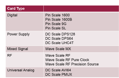
Figure 1. V93000 Cards supported with SmarTest 8

SmarTest 8 features a host of new capabilities that will enable engineers who must deal with highly complex test programs to achieve superior parallelism and throughput. The new software’s many benefits include:

  • Faster test program development
  • Efficient debug and characterization
  • Higher throughput, earlier, due to automated optimization
  • Faster time to market
  • Ease of test-block reuse
  • Efficient collaboration

SmarTest 8 unifies multiple different tools within the SmarTest Work Center (SWC) environment, delivering a state-of-the-art look and feel and an entirely new design to ensure ease of use; see Figure 2.  Let’s take a look at some of the key SmarTest 8 concepts, features and tools that will allow users to reap the new product’s benefits for their test programs.

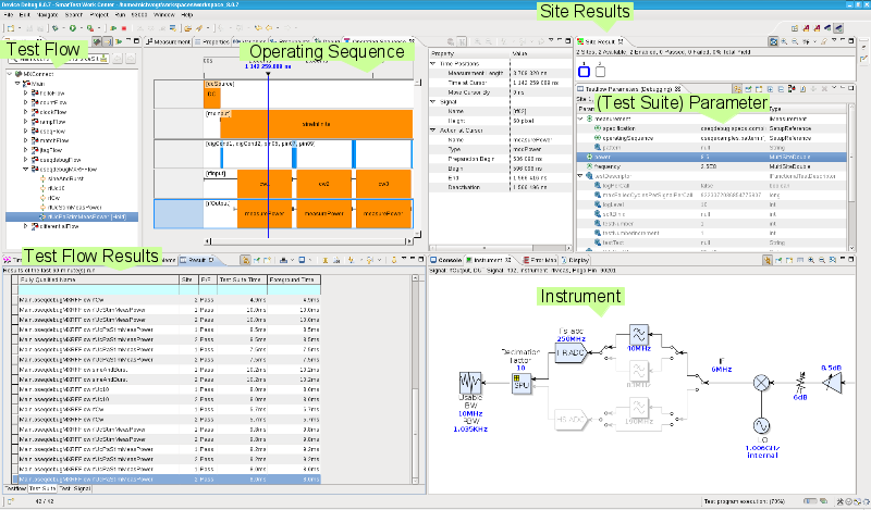
Figure 2. SmarTest 8 comprises a suite of tools designed to simplify and optimize test program development and debug

Operating Sequence
Advanced multi-domain devices consist of multiple different functional blocks. Typical block types include an RF block for transmitting/receiving phone signals, a protocol-ware (PA) interface to condition the device, analog blocks for microphone use and playing music, and/or digital blocks for processing.

Testing one functional block, e.g. the RF block, typically requires ‘assembling a test’ out of multiple pieces, e.g., starting an analog stimulus signal, conditioning the device with digital signals, and starting one or multiple RF measurements. Figure 3 provides an example, with three RF tests displayed in the Operating Sequence View.

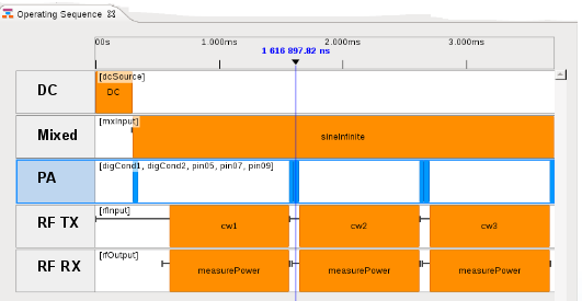
Figure 3. Operating Sequence View, displaying an example RF test

The Operating Sequence is designed to easily assemble the multiple ‘test pieces,’ with precise synchronization where needed. These test pieces are typically patterns, protocol transactions, or ‘actions.’ Actions can be DC stimulus changes (e.g., stepping up a ramp), DC measurements, analog stimulus and measurements, or RF stimulus and measurements – to name some examples.

In addition to easy test setup, the Operating Sequence supports intuitive debugging; the screen view in Figure 3 displays exactly what has been executed.  Interactive changes during debug are well supported – as the second blue block in the figure indicates, inserting an additional transaction into one PA block changes the length of this conditioning block. The SmarTest 8 software automatically ensures that with the next execution of this test, subsequent actions (like cw2 and measurePower in the screen view) are shifted and retain their synchronous start.

Additionally, the Operating Sequence contributes to fast throughput. Multiple measurements can run in parallel, per Figure 3, in which two RF ports are tested concurrently. In addition, the execution of an Operating Sequence is done entirely via the unique test-processor-per-pin hardware of the V93000 system. No software or workstation interaction is required.

Overall, the Operating Sequence, with its new functionality, ease-of-use and optimal throughput, helps enable shorter TTM. This unique tool and concept are unavailable in competitive offerings.

Modular Test Program Structure
Test programs are complex, consisting of up to multiple thousands of tests for the different blocks of the device. The structure of the test setup data of SmarTest 8 is designed to easily deal with this complexity: SmarTest 8 incorporates the concept of subflows. Subflows as part of the testflow tool are established in the ATE software already. SmarTest 8 adds the new component that setup data can be structured and stored in separate and independent ‘subflow’ directories.

This capability enables multiple unique advantages:

  • Teams can work on their own subflows independent from other teams, so collaboration is easy.
  • No manual ‘merge’ effort is needed, as merging of the subflows is automatically performed by SmarTest 8.
  • A complete (proven, debugged) subflow can be reused within multiple test programs of a device family. Reuse here refers to one single source of the subflow, not the ‘copy/paste’ approach typically used today. The latter creates test program maintenance challenges that are prevented with SmarTest 8’s re-use/single-source approach.

By making development and debug faster, easier and far less complex, the modular test program structure ultimately contributes to reduced TTM and time to quality (TTQ).

Test-oriented Use Model via Instruments
Many test systems’ use model is tester- or hardware-centric – it requires the user to learn how to program the tester in order to achieve the needed tasks. SmarTest 8 moves away from this model, allowing the user to focus on the test, not the tester.

With SmarTest 8, the user ‘thinks’ in terms of using instruments for his/her test tasks. Figure 4 shows example instruments and their respective implementations of the tester hardware cards.

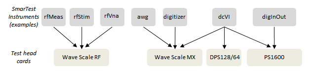
Figure 4. Simplified use model via SmarTest 8 Instruments

These instruments are then programmed via properties and actions; see Figure 5 for an example setup for two VCC signals.

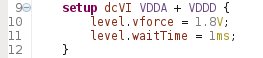
Figure 5. Level specifications for VDDA and VDDD signals

This level specification is identical for all DC instruments in SmarTest 8. When setting up the test, the test engineer will use the level specification for all suitable hardware, which could be a DC Scale DPS128, a parametric measurement unit (PMU) of a Pin Scale 1600 or a PMU of a Wave Scale MX card.

This test-orientation and tester, respectively, hardware-abstraction is consequently used in SmarTest 8, for test setup descriptions, application programming interfaces (APIs), access to results, and in debug tools. This makes the software intuitive and easy to learn, and the test programs are easy to develop, understand and debug, further lightening the burden for the test engineer.

In summary, after several years of development, optimization and beta test, SmarTest 8 is now ‘ready for prime time.’ It is installed at numerous customers, both in test program development and in high- volume manufacturing. SmarTest 8 delivers new benefits that, together with the proven V93000 platform, meets the test needs for the next/newest generation of advanced multi-domain, multi-core ICs. As part of the V93000 platform, it will be continuously expanded to enable even more capabilities and to make test engineers more efficient.

Read More

Posted in Top Stories

W2BI in the Spotlight at Mobile World Congress with New Test Automation Products for the Wireless Market


Advantest, together with W2BI ‒ an Advantest Group company that provides test automation products to help customers quickly launch high-quality smart devices ‒ showcased their newest test platforms for the wireless electronics market at the 2017 Mobile World Congress (MWC) in Barcelona, Spain.

The world’s most expansive exhibition for wireless technology and mobile devices, MWC serves as an annual springboard for many of the next year’s biggest announcements and rollouts of smartphones, tablets and other connected devices. To give you an idea of scale, MWC this year drew more than 108,000 attendees from 208 different countries and boasted approximately 2,300 exhibiting companies.

Within its booth, Advantest featured a suite of products for the mobile communications and Internet of Things (IoT) markets. This included the EVA100 tester, designed for highly efficient evaluation and measurement of analog/mixed-signal ICs, and W2BI’s portable Micro Line Tester (MLT™). This newly introduced system can leverage cloud technology to support testing of LTE-M devices – while effectively lowering the cost of testing smart devices and IoT-based technologies during their development and production life cycles.

MWC provided a valuable forum for Advantest to connect with customers and potential customers to share our perspective on the future of test in the wireless space, and to obtain their thoughts about where IoT test is headed. By most indicators, the space is only going to continue heating up.

Recent market estimates project a whopping 29 billion connected devices by year 2022, and 18 billion connections targeted at wide-area and short-range IoT devices (Figure 1). If we are to capably accommodate this growth, it is critical that the industry address key issues currently challenging wide-area IoT device implementation, including:

  • Lengthy certification process
  • Complex cellular tests used to ensure Safe For Network (SFN) operations
  • Expensive lab equipment for lab testing
  • Non-scalability of test solutions
  • Travel to remote sites to perform live network tests is costly and time consuming
  • Lack of certification knowledge and experience by IoT device makers new to the market

Figure 1. Connected devices are expected to achieve a combined CAGR of 10% between 2016 and 2022. Ericsson Mobile Report November 2016

Some of these challenges can be tackled by simplifying conformance and certification processes, as well as eliminating duplicate tests across the test lifecycle of chips, modules and end products (e.g., wearables, alarm panels, telemetry, and smart homes). Others, however, will require a change in the way the tests are conducted.

W2BI’s new portable all-in-one Micro Line Tester (MLT) platform tackles many of these issues head-on with several key benefits (illustrated in Figure 2):

  • A portable and expandable cloud-managed test platform that reduces time to market;
  • Automation capabilities that have the domain knowledge built in, thus allowing developers to focus on their specific product requirements;
  • Validated industry-standard automated tests downloadable over the cloud directly at the customer site, enabling device pre-certification while reducing travel and lab costs;
  • Pre-defined device profiles to efficiently automate tests across multiple device types (modules, smartphones, IoT products, etc.) without having to customize and adapt tests for each;
  • Ability to expand within a small footprint to adapt to 5G requirements.

Figure 2. W2BI’s portable MLT platform enables onsite testing of mobile devices, greatly reducing test times and costs.


The MLT platform is currently offered in three different modes:

Standalone – Used to conduct ad-hoc tests such as basic device operation, network connectivity, network aggression, data throughput, Voice-over-LTE (VoLTE), SMS, LTE to WiFi handover, and others. The target areas are mainly R&D development processes, and isolation and troubleshooting of post-release device issues.

Developer – Used to create test automation scripts across the network emulator components (radio, packet core, IMS, application server, etc.) and the devices under test, and to collect test metrics for use in analytics. Target areas are primarily QA processes, stress testing, and returns and repair processes.

Conformance – Used to perform automated conformance and certification tests for devices that need to be deployed on wireless networks in accordance with industry standards or operator-specific requirements. The target areas are mainly pre-certification tests, network safe tests, and conformance tests.

W2BI’s MLT platform is currently deployed at a US Tier-1 wireless operator, performing conformance tests on smartphones, and IoT modules and products. The Micro Line Tester is also undergoing multiple trials across test labs, module manufacturers and smartphone OEMs using both the standalone and developer modes. Shipment volume is expected to pick up toward the second half of 2017, when mobile operators begin fully deploying LTE-M and NarrowBand IoT (NB-IoT) on their networks.
As W2BI continues to develop new products that help to enable the growth of the mobile device market, expect to see technologies and products that address new protocols, including LTE-M and NB-IoT, called a game changer for the IoT industry because it extends LTE’s market reach. By allowing LTE to cost-effectively support lower data-rate applications, LTE-M is being touted as a good fit for low-power sensing and monitoring devices such as health and fitness wearables, utility meters, and vending machines, among others.


Read More