By Zain Abadin, Director, Handler Product Engineering and Marketing, Advantest
The amount of electronic content in automobiles continues to grow at a brisk pace, and sensors represent a significant percentage of cars’ electronics. MarketsandMarkets estimates that the automotive sensors market alone will reach US$36.42 billion in value by 2023, at a compound annual growth rate (CAGR) of 6.7 percent between 2017 and 2023.
Sensors in cars are used to monitor and control a host of functions. Pressure sensors are growing at nearly the same rate as the overall automotive sensor market. Technavio reports that the global automotive pressure sensors market is anticipated to post a CAGR of more than 6% between 2017 and 2021. This is due to growing demand for fuel efficiency, safety, and reduced emissions. Many different types of pressure sensors exist, with varying requirements as to the level of pressure they require.
One key subset of pressure sensors – exhaust and side and center airbag sensors – requires very low pressure. The thresholds at which they should activate and deploy are well below 1 megapascal (MPa), and as low as 600 kilopascal (0.6MPa) because their ability to deploy when needed is absolutely critical to protect passengers’ health and safety. Therefore, it’s imperative that they be accurately tested to ensure their functionality prior to purchase and use of the vehicle into which they’re integrated.
The traditional test flow for these sensors is done at the wafer level, conducting logic and DC test on the sensor ASIC first, then performing DC test separately on the sensor element, i.e., the part of the logic device that will make the sensor actually deploy. Normally, these tests are performed separately, then the ASIC and element are tested again as a unit, utilizing manual handling to move the sensors between test steps. This includes a range of temperature tests, which are essential to ensure desired functionality regardless of whether the car is being driven in Palm Spring in the summer or Minnesota in the winter. The multiple steps and manual handling associated with the typical test approach impact test time and cost, and can delay time to market (TTM) for the carmaker.
New solution eases pressure on users
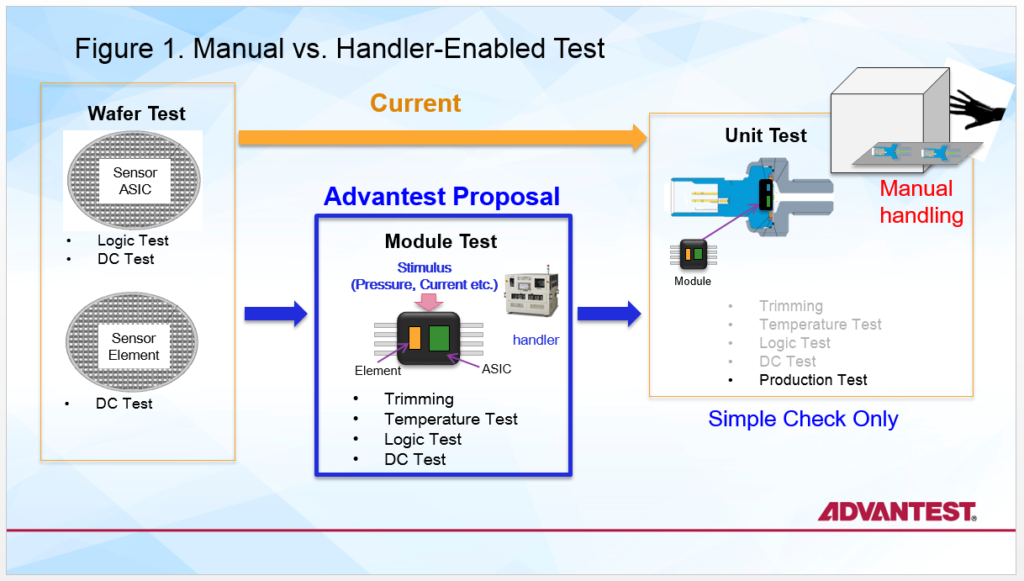
Advantest proposes a new approach, combining a stimulus test cell with an automated handler, creating a module that can accommodate trimming, temperature, logic and DC test all in one unit. Once these are complete, all that is left is to install the module and perform a quick production test to ensure the module is installed properly. This solution allows the user to omit several individual tests and perform the necessary tests in one solution, all at the same time.

Figure 1 illustrates the difference between the current methodology and the Advantest solution, which combines a test handler and EVA100 measurement system with an HA7200/7300 temperature and pressure stimulus unit. Together, they create a compact and easy-to-use production-volume test environment.

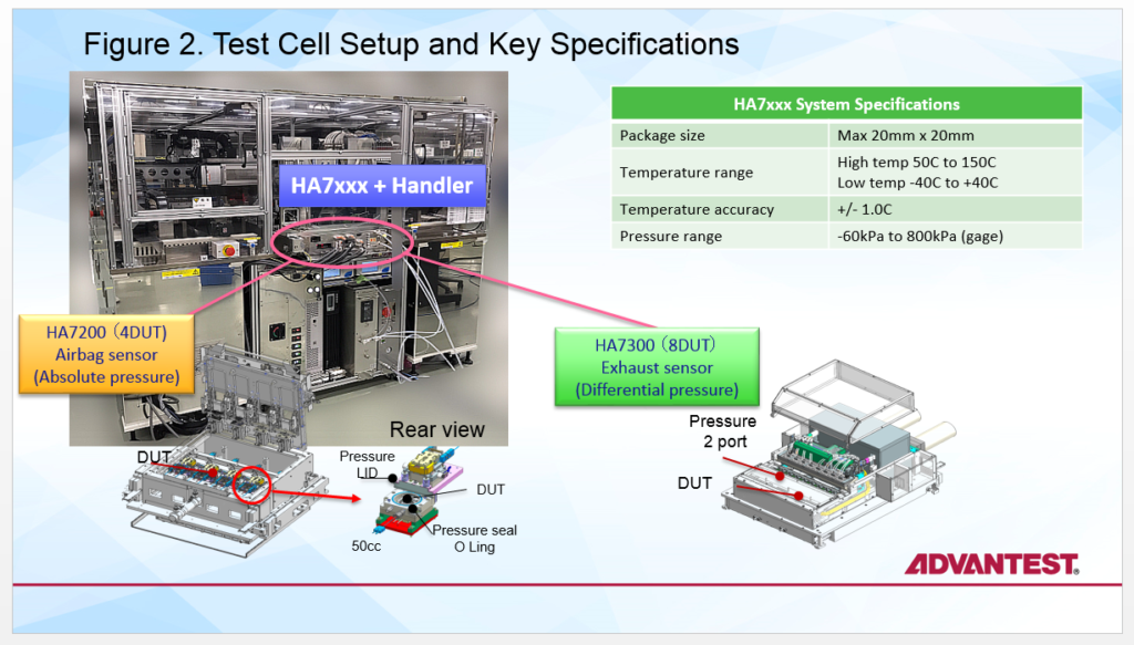
Figure 2 shows the test cell setup, which is basically the same regardless of the desired pressure unit. The HA7200 can measure absolute pressure on up to four devices under test (DUTs), which is the ideal choice for airbag sensors. The HA7300 is designed for testing differential pressure sensors (e.g., exhaust sensors), whose use is becoming more pervasive as vehicle designs continue to focus on improving fuel economy and reducing hazardous emissions. The HA7300 enables accurate application of two separate pressures within a short time, using two ports, and can test up to eight DUTs. The setup is flexible, similar to a rack, so the pressure modules can be easily swapped out to test both types of pressure sensors. Figure 2 also includes some of the key specs associated with the setup – notably, the wide range of temperatures and pressures that can be accommodated, and the associated high degree of accuracy that can be attained.
Two major benefits of the Advantest stimulus solution are its ability to perform temperature and pressure test simultaneously, and to minimize the stability time for both. This is due to the use of dual fluid active thermal control (DF ATC), which works together with the conduction employed in the unit to maintain device temperature.
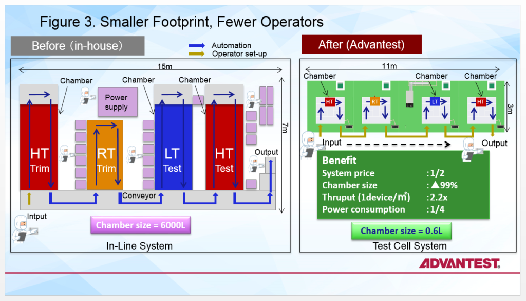
In the automotive market, testing and specifications are highly restrictive – because public safety is parament, the test levels are set, and then performed over and over. There is no margin of error, which means these is no sampling; every device must be tested. This has led to test houses creating their own custom solutions, which are costly. As Figure 3 shows at left, four setups are required for the in-house solution, necessitating a very large footprint. In addition, multiple operators are needed due to manual handling, which is a drain on time and resources.
Devices are trimmed first at high temperature (HT) and high pressure, next at room temperature (RT), and then they are tested at low temperature (LT), after which they are brought back up to HT and tested again prior to output. This means the device is heated or cooled to the desired temperature, then brought to the tester. However, during transport, the device temperature shifts by some degrees before it is tested.

At right in Figure 3, is the process enabled by the Advantest test cell system. The setup includes the same number of tests, but because it based on the use of a handler, the DF ATC technology and pressure sensor module with much smaller chambers, the system footprint is considerably smaller than that of the in-house approach. Also, because the test cell uses conduction rather than convection, the device is always in contact, ensuring the desired temperature is accurately maintained – simultaneously with the pressure. With this approach, system cost is cut by about half, power consumption is reduced by 25 percent, and operator resources are used much more efficiently.
Looking ahead – to the current sensor
Another automotive sensor challenge for which a new test approach will soon be needed is related to current sensors used in electric vehicle (EV) batteries and motors. New batteries and motors will be much larger, and the current needed to test these sensors may exceed 1000 amps (A), while accommodating the requisite wide ranges of temperature – within an acceptable guard band.
In order to test such current sensors under the 1000 A application condition, sufficient heat generation measures and safety measures are required, so huge test and stimulus equipment is required. Therefore, a method of applying a magnetic field at module level instead of applying a current at unit level is desired to realize a small equipment. However, it is a big technical challenge to apply magnetic flux uniformly while maintaining temperature.
Together, these challenges have created major hurdles that the test industry needs to address. Thanks to increased regulation, demand for electric vehicles is on the rise – Technavio anticipates a CAGR of 42% for current sensors, with the market reaching $87 million by 2021. Meeting this demand will require better and faster testing of current sensors than is being done today. Advantest is leveraging its expertise in sensor testing to investigate new advanced solutions. We look forward to sharing the results of these efforts with you in the near future.
Read More


 Doug Lefever, Director, President and CEO of Advantest America, and Managing Executive Officer, Board of Directors, Advantest Corporation