Pages Menu
Categories Menu

Posted in Q&A

Q&A Interview

Doug Lefever, Director, President and CEO of Advantest America, and Managing Executive Officer, Board of Directors, Advantest Corporation

By GO SEMI & Beyond staff

This article was adapted from an interview that originally appeared in the Silicon Catalyst newsletter.

Q: Where does Advantest fit into the semiconductor ecosystem?

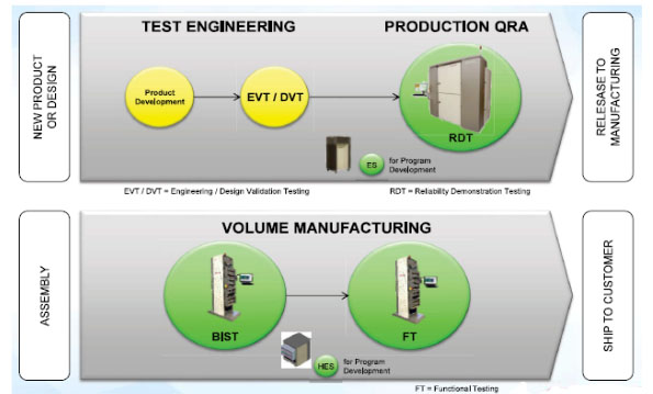
A: As the semiconductor industry has evolved and grown, so has Advantest. We are active throughout the ecosystem, as the figure shows, providing solutions from silicon-level testing up to system-level testing – an area we see having a great deal of potential for growth. Today, our industry-wide involvement reaches beyond our core capabilities in test and measurement to encompass lithography, data logging, consulting and other areas. Oftentimes, folks at startups have done engineering development, but have not been involved in broader business operations, so Advantest can help to bring them along the learning curve. This allows us to form alliances with early-stage companies, which typically don’t need a deep dive into test technology or to get a device onto a tester.

Q: Why does Advantest partner with an incubator like Silicon Catalyst?

A: Because Silicon Catalyst is focused solely on semiconductor solution startups, it provides very early-stage companies with access to goods, services and experience from its network of in-kind partners – all of which are businesses that have been through the startup process. At Advantest, we’re excited to be able to support new startups through our involvement with the incubator. Our commitment comprises 160 hours per month technical education, management guidance, sharing insights and mentoring – the equivalent of one month’s work by a full-time, experienced industry member.

I want to stress that, as these are very, very early-stage ventures, none has yet implemented our actual test resources on its nascent IC designs. We are mentoring and advising them on developing test strategies and manufacturing flows – and, on a broader scale, we are sharing our hard-won experience in running a company. Our business proficiency allows us to perceive where young ventures have weaknesses and help them to address those weaknesses.

These young companies have promising technologies or application ideas, but generally need to gain “ground floor,” startup-level experience. Silicon Catalyst provides opportunities for them to begin building out their teams and to make real connections with equipment and technology providers or financial people, depending upon their stage of development. A key reason that we decided to join the ecosystem is so that we can help figure out ways to reduce the cost of developing and financing new semiconductor startups; funding new technology or anything semiconductor-related has proven challenging to the industry.

We recognize that we’re not going to be selling test systems right away. But a few years down the road, as some portfolio companies that have had access to our technology and our support services become successful, they may gravitate toward our platforms. Advantest does not fund any of these companies or sit on their boards, but we are the only ATE company that gets to help evaluate new companies and new technologies when they ask to join Silicon Catalyst. We can also talk to companies with technologies or IP of interest to us, regardless of whether or not they are added to the portfolio.

Gaining exposure to what’s coming gives us insight into where our industry is headed, what type of equipment customers will need and, perhaps, even the types of performance we might expect from future electronic products. We are gleaning information about emerging technology trends, as well, in such areas as optical, materials, power management, memory cells, MRAM, and low-power memory technology – to name a few.

Q: Where are you seeing momentum in semiconductor startups?

A: As I mentioned, optical is a key trend – many optical-related companies are leading the next wave of high-bandwidth connectivity and low-power computing. While some are building a single chip and others are developing whole modules, the volume of optical products is starting to grow, and high-volume manufacturing (HVM) will be the next step.

In terms of applications, consumer optical-based communications are on the rise. In this area, a new standard is emerging called NGPON-2, which is next-generation Ethernet over passive optical connections. Another area of focus of a number of startups is high-bandwidth computing, while massively parallel computing is enabling advances in artificial intelligence (AI), machine learning and Big Data with shared databases. Dedicated chips are being built for machine learning.

Wearable technology for medical and health-related applications is increasingly incorporating such capabilities as blood monitoring and analysis. One company is making a device that will be able to perform a diagnostic screening on a blood sample at point-of-care without requiring an extensive blood panel analysis. The AI system will be taught patterns consistent with specific pathogens, bacteria or other components so that, when the blood sample is put into the device, the system can determine, within 10 minutes, what’s in there – a much faster and cheaper solution than what’s available today.

Other interesting areas addressing power requirements include low-power memory and energy harvesting, which is wearable technology that uses the heat of your body to charge a battery. The bigger the temperature difference between your body and ambient air, the more energy it puts out.

These are just a few of the technology areas where we are seeing burgeoning opportunities for startups, as well as the industry at large, in the semiconductor arena.

Read More

Posted in Top Stories

Automated Pick-and-Place Handler Enables Test Engineering Efficiency in Lab Environment

By Zain Abadin, Director, Handler Product Engineering and Marketing, Advantest

In the laboratory environment, the principal goal is to complete development and pre-production testing of integrated circuits (ICs) as quickly and cost-effectively as possible. An associated challenge is to ensure that tester and operator resources are utilized efficiently so that testing can be completed on or ahead of schedule, further improving time to market (TTM).

The typical test approach is to have an operator manually load the devices into the test sockets, and then run the specific test for the defined time per the device maker – this could range from 5 seconds to 30 minutes or more per device. The actual number of devices also varies; in pre-production, there may be as many as 10 trays, containing a few hundred ICs. Testing in this manner is an inefficient use of labor, engineering, and tester resources. For short test times, this means an operator sitting by the tester to load/unload devices under test (DUTs). For long test times, the operator inserts a device and moves to another task on the floor. If an operator isn’t immediately available to change the DUT, the test process can be extended or delayed, causing it to take longer time to complete the lot and increasing the cost of test and TTM.

A scalable handler that can be used for both ATE and bench testing is the ideal solution to these challenges, allowing development and pre-production testing for a variety of device types and batch sizes to be completed faster, and enabling devices to be sent to market in a timelier manner. The result is a significant savings in both labor and cost of test.

Advantest’s M4171 handler delivers an efficient solution to meet the mobile electronics market’s needs for cost-efficient, thermally controlled IC testing. The unit is small – about one-quarter the size of other handlers – making for a small footprint and easy docking. The single-tray handler utilizes one contact arm to pick up a device from the tray and places it into the socket. Once the device has been tested, the same arm moves in to pick up the device and place it into its post-testing position in the tray.

Flexible operation equals faster results

The M4171 was created with a range of features intended to enhance lab efficiency (Figure 1). These features are summarized below.

Remote accessibility/control from any location

To run tests locally on the handler, the operator is on site to load the trays of DUTs, run the automated test process and remove the trays when testing is complete. However, when the operator’s workday has ended, there will be handler/tester downtime until the next shift or the next day. The M4171 includes cameras that allow a team member at another location, anywhere in the world, to not only monitor activity and view results remotely, but also to actually operate the handler remotely (Figure 2).

This means that the handler can be run at any time of day – a team member located across the country or across the globe can access the handler during his or her workday, moving, docking and undocking the handler, and running the desired tests. In turn, this allows companies to spread out their global resources and schedule operation so that there is less equipment downtime, i.e., a higher utilization rate. Testing can thus be completed faster, speeding TTM.

Multi-mode testing to expedite the test process

It can run multi-mode test processes, both pre-defined and user defined, including automated testing, automatic ID testing, output tray re-testing and manual testing (Figure 3).

High accuracy cycle temperature across wide temperature range

In addition to its automated device handling and remote operation, the M4171 is unique due to its wide-temperature sensor-based thermal-control capabilities, which range from -45° C to 125° C.  The M4171’s tri-temp technology enables operation of the handler over a broad range of temperatures.  The system uses direct device-surface contact, which enables quick temperature switching for fast ramp up and ramp down. With this capability, ramp-up, soak time, ramp-down and time-at-temperature can be set up all at once, and run one after the other.

The handler collects data continuously throughout the process, enabling significant time and resource savings (Figure 4). In fact, cycle temperature testing time can be reduced by more than 40 percent compared to manual thermal-control solutions.

Flexible bin assignment for output

A unique capability of the handler is that it enables pre-programmed binning within the output tray – once the handler and tester are docked, the tester can tell the handler into which bin a device should be placed. This allows the customer to utilize different binning approaches for different devices or batches, to pause in the test process or specify retesting. As Figure 5 shows, the user can define bins within the tray as pass, fail, retest, empty row, etc. – whatever lab functions are desired.

A label or category can also be assigned to a device within the trays, and that label stays with the device throughout the test process. With this capability, the customer can easily tell the devices apart by tray section – which passed, which failed, which need to be retested, etc. This is vital to ensure rapid transition between batches, or from the lab environment into pre-production.

Fully compatible with the V93000 and T2000 platforms as well as other testers, the M4171 also features a 2D code reader, a device rotator and a high-contact force option.  In addition, users can quickly convert the handler to accommodate different setups – with only a few parts to change, conversion takes just 10-15 minutes compared to 30 minutes or more on other handlers. Key specifications for the handler are shown in Figure 6.

A cost analysis using an example test time of 120 seconds and a quantity of 20 testers reveals that using the handler enables a 69-percent reduction in cost. Not only can each operator handle more units per hour and more test cells, but the customer has the flexibility to test triple the number of units using the same number of tester (Figure 7).

The M4171 is available now, providing integrated device manufacturers (IDMs) and outsourced semiconductor assembly and test companies (OSATs) with a compact, cost-efficient engineering test solution that delivers both thermal control and automated device handling.


Read More

Posted in Top Stories

Speedier, More Accurate Testing of Automotive Sensors Is Here

By Zain Abadin, Director, Handler Product Engineering and Marketing, Advantest

The amount of electronic content in automobiles continues to grow at a brisk pace, and sensors represent a significant percentage of cars’ electronics. MarketsandMarkets estimates that the automotive sensors market alone will reach US$36.42 billion in value by 2023, at a compound annual growth rate (CAGR) of 6.7 percent between 2017 and 2023. 

Sensors in cars are used to monitor and control a host of functions. Pressure sensors are growing at nearly the same rate as the overall automotive sensor market. Technavio reports that the global automotive pressure sensors market is anticipated to post a CAGR of more than 6% between 2017 and 2021. This is due to growing demand for fuel efficiency, safety, and reduced emissions. Many different types of pressure sensors exist, with varying requirements as to the level of pressure they require.

One key subset of pressure sensors – exhaust and side and center airbag sensors – requires very low pressure. The thresholds at which they should activate and deploy are well below 1 megapascal (MPa), and as low as 600 kilopascal (0.6MPa) because their ability to deploy when needed is absolutely critical to protect passengers’ health and safety. Therefore, it’s imperative that they be accurately tested to ensure their functionality prior to purchase and use of the vehicle into which they’re integrated.

The traditional test flow for these sensors is done at the wafer level, conducting logic and DC test on the sensor ASIC first, then performing DC test separately on the sensor element, i.e., the part of the logic device that will make the sensor actually deploy. Normally, these tests are performed separately, then the ASIC and element are tested again as a unit, utilizing manual handling to move the sensors between test steps. This includes a range of temperature tests, which are essential to ensure desired functionality regardless of whether the car is being driven in Palm Spring in the summer or Minnesota in the winter. The multiple steps and manual handling associated with the typical test approach impact test time and cost, and can delay time to market (TTM) for the carmaker.

New solution eases pressure on users

Advantest proposes a new approach, combining a stimulus test cell with an automated handler, creating a module that can accommodate trimming, temperature, logic and DC test all in one unit. Once these are complete, all that is left is to install the module and perform a quick production test to ensure the module is installed properly. This solution allows the user to omit several individual tests and perform the necessary tests in one solution, all at the same time.

Figure 1 illustrates the difference between the current methodology and the Advantest solution, which combines a test handler and EVA100 measurement system with an HA7200/7300 temperature and pressure stimulus unit. Together, they create a compact and easy-to-use production-volume test environment.

Figure 2 shows the test cell setup, which is basically the same regardless of the desired pressure unit. The HA7200 can measure absolute pressure on up to four devices under test (DUTs), which is the ideal choice for airbag sensors. The HA7300 is designed for testing differential pressure sensors (e.g., exhaust sensors), whose use is becoming more pervasive as vehicle designs continue to focus on improving fuel economy and reducing hazardous emissions. The HA7300 enables accurate application of two separate pressures within a short time, using two ports, and can test up to eight DUTs. The setup is flexible, similar to a rack, so the pressure modules can be easily swapped out to test both types of pressure sensors. Figure 2 also includes some of the key specs associated with the setup – notably, the wide range of temperatures and pressures that can be accommodated, and the associated high degree of accuracy that can be attained.

Two major benefits of the Advantest stimulus solution are its ability to perform temperature and pressure test simultaneously, and to minimize the stability time for both. This is due to the use of dual fluid active thermal control (DF ATC), which works together with the conduction employed in the unit to maintain device temperature.

In the automotive market, testing and specifications are highly restrictive – because public safety is parament, the test levels are set, and then performed over and over. There is no margin of error, which means these is no sampling; every device must be tested. This has led to test houses creating their own custom solutions, which are costly. As Figure 3 shows at left, four setups are required for the in-house solution, necessitating a very large footprint. In addition, multiple operators are needed due to manual handling, which is a drain on time and resources.

Devices are trimmed first at high temperature (HT) and high pressure, next at room temperature (RT), and then they are tested at low temperature (LT), after which they are brought back up to HT and tested again prior to output. This means the device is heated or cooled to the desired temperature, then brought to the tester. However, during transport, the device temperature shifts by some degrees before it is tested.

At right in Figure 3, is the process enabled by the Advantest test cell system. The setup includes the same number of tests, but because it based on the use of a handler, the DF ATC technology and pressure sensor module with much smaller chambers, the system footprint is considerably smaller than that of the in-house approach. Also, because the test cell uses conduction rather than convection, the device is always in contact, ensuring the desired temperature is accurately maintained – simultaneously with the pressure. With this approach, system cost is cut by about half, power consumption is reduced by 25 percent, and operator resources are used much more efficiently.

Looking ahead – to the current sensor

Another automotive sensor challenge for which a new test approach will soon be needed is related to current sensors used in electric vehicle (EV) batteries and motors.  New batteries and motors will be much larger, and the current needed to test these sensors may exceed 1000 amps (A), while accommodating the requisite wide ranges of temperature – within an acceptable guard band.

In order to test such current sensors under the 1000 A application condition, sufficient heat generation measures and safety measures are required, so huge test and stimulus equipment is required. Therefore, a method of applying a magnetic field at module level instead of applying a current at unit level is desired to realize a small equipment. However, it is a big technical challenge to apply magnetic flux uniformly while maintaining temperature.

Together, these challenges have created major hurdles that the test industry needs to address. Thanks to increased regulation, demand for electric vehicles is on the rise – Technavio anticipates a CAGR of 42% for current sensors, with the market reaching $87 million by 2021. Meeting this demand will require better and faster testing of current sensors than is being done today. Advantest is leveraging its expertise in sensor testing to investigate new advanced solutions. We look forward to sharing the results of these efforts with you in the near future.


Read More

Posted in Top Stories

Preparing Solid-State Drives for Qualification Testing

By Vishal Devadiya, R&D Applications Engineer, Advantest

The market for solid-state drives (SSDs) remains strong. International Data Corp. (IDC) recently released figures forecasting a five-year compound annual growth rate (CAGR) of 15.1 percent in worldwide SSD unit shipments with SSD industry revenue expected to reach $33.6 billion in 2021. With SSD usage growing in PCs, consumer electronics and other applications, qualification testing has become increasingly critical as has finding ways to make the process faster and less costly so that SSDs can be brought to market more quickly.

Qualification testing, in essence, is a formally defined series of tests for evaluating a component or system to ensure its functionality, robustness and reliability prior to final approval and acceptance for release to production. Three types of qualification tests must be performed on SSDs before they enter the manufacturing phase:

  1. Engineering verification test (EVT) and
  2. Design verification test (DVT), both of which are run on a number of samples to check a SSD’s functionality, typically taking one to two weeks; and
  3. Reliability demonstration test (RDT), which is run on every device (not just samples) to check each SSD’s reliability and data integrity. RDT is run for a minimum of 1,000 hours and involves thousands of drives.

What is required to prepare an SSD for qualification testing? It is essential to make sure there are no functionality issues with the drive – most importantly, that it powers up correctly, and then that it works as expected in terms of running input/output (I/O) operations. If any issues arise, finding and fixing the root cause must be achieved as quickly as possible to avoid time-to-market (TTM) delays.

Several key issues can arise during the preparation process. Power-up failure, the most serious, typically happens because of a link training issue. This problem generally applies to PCIe drives because the PCIe protocol is quite complex with different layers in the architecture. Another issue is link retrain/drop. In this instance, the system may power up properly, but essentially becomes stuck in a non-ready loop shortly thereafter. A third type of problem is failure during I/O operations, which comprises three types of failures: write, read or data compare (write/read don’t match).

If one of these issues is discovered during preparation, the problem must be debugged. Traditional debugging methods are less than satisfactory. One way is to perform analysis on the available logs from the host and the drive, but the logs provide few details useful for analysis. The more typical approach is to use a protocol analyzer (PA) to capture bus trace and perform analysis to link issues (see Figure 1).

Figure 1. A PCIe analyzer on an engineering tester

But using a PA for this purpose has its own challenges:

  • The issue may not occur on a fixed slot number on the tester. If the test is run on a DVT trace during DVT and the issue occurs on the first device under test (DUT), the problem can only be captured if it is reproducible and consistent to that DUT slot.
  • If this does not work, it may be necessary to connect multiple PAs to avoid having to keep moving the PA from slot to slot. This creates a huge time sink and adds cost.
  • The large interposer required to connect the PA to the tester may temporarily change the signal properties, which can mask the issue from the tester and prevent its discovery.
  • Ongoing DVT testing on other DUTs cannot be interrupted or stopped in order to debug. EVT takes a week and RDT requires at least 1,000 hours. If an issue occurs within these time periods and a device in a specific slot experiences a failure, testing on all devices must be stopped so that the PA can be connected to that specific slot and then started up again following a period of downtime.
  • Thus, it becomes necessary to reproduce the issue. If there are insufficient or no data logs and a protocol trace must be captured, the test must be rerun. If it is not consistent, reproduction can be difficult, if not impossible. If a failure that happened at 120 hours initially does not happen again, the cause cannot be determined.
  • Additional considerations arise if the test is running under a thermal environment. Some SSD manufacturers run devices at a high temperature during RDT; if an issue arises, there is no way to connect a PA.

The bottom-line impact of these challenges is that it takes longer to identify the issue, resulting in delayed TTM and loss of revenue. One solution is to use the traffic capture tool created by Advantest and available as an add-on to the proven MPT3000 platform for system-level testing of SSDs.

The traffic capture tool enables transaction layer packet capture and link training/status state machine (LTSSM) capture, both of which are critical for debugging, as the following example illustrates. The tool also captures submission and completion queue information for each command and performs a command log dump to assess the number of commands issued and completed. Essentially, the traffic capture tool captures whatever is going on the bus between the FPGA-based test system and the DUTs.

The following figures illustrate how the traffic capture tool detects a power-up failure. In Figure 2, the link is good, but there is an error on the last line of code, indicating that the block device is not present. This means the device did not get ready within 120 seconds and thus timed out.

Figure 2. The drive linked up successfully, but did not get ready within the specified timeout.

Figure 3. The highlighted lines of code indicate that the SSD never got ready.

In Figure 3, the transaction layer packets (TLP) capture screens indicate that the device kept repolling and returning a value of 0 until hitting the 120-second mark. This means the device did not get ready (CSTS.RDY) and experienced a power-up failure. Once the failure is correctly identified, the information is relayed to the SSD manufacturer, whose challenge is to determine why the failure occurred.

When selected as an option, Advantest’s traffic capture tool runs continually in the background on the MPT3000 platform – essentially as an in-line process, capturing data that may be needed to rerun a test or reproduce an issue. Using the traffic capture tool on the tester allows the user to:

  • Run tests on all slots at the same time and capture the information required to debug issues;
  • Capture the traffic log at the time of the failure without having to reproduce the issue; and
  • Change the amount of logic in the design to capture more information if required. Because the test system is FPGA-based, it is easy to adjust the amount of logic for data capture.

The bottom-line benefit is earlier identification and resolution of device issues, resulting in the faster TTM that device makers require to keep pace with continuing market growth.


Read More

Posted in Top Stories

SmartShell – A Unique Software Interface for Design and Production

By Shu Li, Business Development Manager, Advantest America and Michael Braun, Product Manager, Advantest Europe

Before device test can take place on automated test equipment (ATE), device-specific test programs need to be developed for the target device and test system. As part of this process, a large amount of digital test content (patterns) gets translated from EDA (design/simulation) to ATE (test) format and needs to be debugged and characterized on the target tester.

In the mixed-signal (MX) and radio-frequency (RF) domain, scripts in various languages (tcl, Python, LabView, etc.) are often used for device bring-up and characterization on bench instruments, using early device samples on an evaluation board, either before ATE test program development starts or sometimes in parallel.

These often interactive scripts are not natively applicable to the production test system, so ATE users have developed proprietary solutions to bridge the gap between ‘bench type’ engineering test and production test environments. This enables leveraging some of the early device learnings for volume testing, or simply running the same test scripts in the two very different environments.

Both digital pattern validation and MX/RF script execution or conversion to ATE have potential for improvement and standardization, which will benefit both time-to-market (TTM) and time-to-quality (TTQ). This article will provide further details for both areas.

Digital (DFT) pattern bring-up and validation

Test patterns for scan, built-in self-test (BIST), functional, or other digital tests are typically created by design or DFT engineers in their design/simulation (EDA) environment and then handed over to the test department, where they are converted to the native ATE pattern format and integrated into the production test program. As part of this process, all patterns need to be validated and characterized on the tester, to make sure that they work as intended and have enough margin to guarantee a stable production test.

This pattern bring-up and validation process can be very time consuming because initial pattern generation and bring-up/validation is typically done in two very different environments: design/DFT/simulation versus test engineering. The design or DFT engineer creates the test patterns, but it is the test engineer’s responsibility to convert and run them against the actual silicon. If they don’t work, the test engineer will produce a log file with failing cycles for the pattern at hand and send it to the designer, whose task is then to identify the root cause of the failures in the simulation environment and to re-generate a corrected test pattern as needed. The corrected pattern needs to be translated and validated on the tester again, going back and forth between design and test. Often, design/DFT and test engineering are isolated from each other, in two different locations, communicating by email or FTP. The test engineer will thus notify the DFT engineer of discovered errors, but the latter may not get around to re-simulating the test patterns immediately. As a result, the test development process will incur some delays. The majority of patterns may pass, but some tricky ones can take months of re-spins, which will not help with getting working products to market quickly. This traditionally manual process – offline pattern generation, conversion and download, then emailing feedback about errors – is painful and time consuming (Figure 1).

If there were a way to execute and validate the generated patterns directly from the DFT/simulation environment without going through the full circle of pattern translation and fail cycle collection for every minor change, it would benefit all parties involved and reduce the pattern bring-up cycle time.


Figure 1. The debugging process involves lengthy communication between design and test, requires significant learning, and is prone to errors, leading to lengthy cycle times.


Scripts for mixed-signal/RF ‘bench instrument’ test on ATE

Mixed-signal and RF testing involves, besides some digital resources to set up and control the device, additional analog and RF instrumentation. In a lab environment, these resources are benchtop instruments such as oscilloscopes, spectrum analyzers, waveform generators and other tools.On the bench, each test requires specific control scripts for both the device and the various lab instruments involved. On the ATE system, fully integrated hardware instruments are used and controlled by standardized software components that are part of a generic test program. Often, bench instruments have a higher precision for specific tasks but are not as universal as ATE resources and cannot reach nearly the same throughput as ATE can deliver. For volume data collection in characterization, significant effort must be made to reach high throughput for data collection from many devices in a reasonable amount of time. Leveraging an ATE to do some tasks that are normally done in the lab/bench environment will speed up this data collection significantly and help to smooth the transition between design/bench and ATE. In this context, it would be very helpful to have a solution that allows moving back and forth seamlessly between the lab/bench environment and the ATE, without the need to convert bench-type scripts into ATE ‘native’ test programs. Running the exact same script(s) on the bench AND on the ATE system would help to improve correlation and TTM, while leveraging knowledge from both environments.

Figure 2. Time to market is a major issue when dealing with scripting for mixed-signal/RF devices. Producing a working customer sample can take 9-12 months, depending on chip size, type, etc.

Building a unified interface to bridge between design and test

What’s needed to address these challenges is an easy-to-use client/server environment that simplifies the communication between design and test to enable smart debugging. Advantest has developed a software option for its V93000 system-on-chip (SoC) test system that provides such a solution.

The newly developed SmartShell is a software environment for digital pattern validation and native script execution on ATE. The interface links directly between the DFT/bench environment and the V93000 tester, without the need to convert patterns and scripts to the tester’s ‘native’ data format. This allows fast pattern bring-up and characterization, enabling DFT engineers to validate their patterns faster and designs to be characterized more efficiently before they are released to production on the V93000 system. The block diagram in Figure 3 illustrates the dataflow process.

Figure 3. SmartShell data flow, from pattern/script generation to ATE and back.

With this new tool, porting different test content is made easier and straightforward, giving designers the freedom to incorporate various tasks into their test program without having to think about how to port them to an ATE system. Those that work best for the device being developed will be converted when it comes to manufacturing.

Engineers in both design and test can use the tool. The DFT engineer can run a simple script instructing the tool to check a new pattern or to loop over a number of patterns while varying conditions like voltage or frequency. He or she can access the results directly from their environment, without having to learn the native formats and software environment of the test system. The test engineer can run scripts originally generated for a totally different environment, and then quickly compare ATE results with results from the bench instrumentation. The command interface controls functionality and execution, and allows the results to be viewed in the engineer’s preferred format (see Figure 4).

Figure 4. The software package features an interface that is easy to use for design and test engineers alike.

SmartShell’s key capabilities include:

  • On-the-fly control of tester resources for digital, mixed-signal, RF and DC measurements
  • Fast internal pattern conversion, execution, and back-propagation of results
  • Ease of programming using any command-based script language
  • Accommodates customized script language using a bridge to its standard set of commands
  • Auto-recording/generation of setups for early production to ensure reusability
  • Compatible with SmarTest 7 (DFT/pattern validation only) and SmarTest 8 (Scripting)

Summary

SmartShell represents a solution to bridge the gap between design and test, delivering capabilities for pattern validation and script execution that are beneficial regardless of company size or device type. Early validation can be done in a well-contained design or bench environment, without the need to ‘learn the tester.’ The highly programmable SmartShell interface for the V93000 allows experts to best utilize their individual skillsets to debug devices effectively and efficiently in a highly integrated manner. The tool significantly shortens the turnaround times for high-quality test patterns and scripts, enabling device makers to achieve both faster TTM and lower overall cost of test.

Read More