Pages Menu
Categories Menu

Posted in Uncategorized

In Vivo Skin Imaging Technology Developed to Aid in Early Diagnosis

 Advantest has developed a non-invasive method to achieve real-time 3D imaging of the vascular network and blood condition (oxygen saturation) of the living body, using a photoacoustic method to detect ultrasonic waves generated by laser irradiation. This method may be used for early diagnosis and monitoring of physical functions related to beauty and health.

As part of the “Innovative Visualization Technology to Lead to Creation of a New Growth Industry” project operated by Advantest’s Takayuki Yagi under the auspices of the Impulsing Paradigm Change through Disruptive Technologies Program (ImPACT), a program of Japan’s Council for Science, Technology and Innovation, an R&D group led by Professor Yoshifumi Saijo of Tohoku University and Noriyuki Masuda of Advantest has succeeded in developing in vivo skin imaging technology (1) that can simultaneously generate dual-wavelength photoacoustic images and ultrasound images.

Photoacoustic imaging is a method of imaging the interior of a living body by irradiating light into the body and measuring ultrasonic waves generated from blood or tissues that selectively absorb light energy. It is attracting interest as a new noninvasive imaging method suitable for measuring small blood vessels in the skin, which is difficult with conventional imaging techniques.

However, when using only photoacoustic imaging, even if microvessels in the skin measuring several tens of microns or less in diameter are imaged, it is impossible to ascertain which region of each layer in the skin they are in. In addition, it is possible to photoacoustically measure the oxygen saturation level of blood vessels (3) by using light sources of multiple wavelengths, but the movement of living bodies affects measurement results, so the use of this method has hitherto been limited to research applications such as animal experiments.

The newly developed in vivo imaging technology utilizes a focused ultrasonic sensor that can detect multiple ultrasonic signals. Thus, photoacoustic waves and ultrasonic waves can be measured with the same sensor, while signals are generated on two alternating wavelengths, allowing the detection of ultrasonic waves that image the microvascular network in the dermis as well as blood oxygen saturation (Fig. 1). A 6 mm square area of 2 mm depth can be imaged in about 4 minutes. Also, using the acquired data, mapping of oxygen saturation and the superposition of photoacoustic images and ultrasound images is possible.

Biopsy studies have proved that signs of skin aging such as spots and wrinkles are related to microvessels in the skin. The newly developed photoacoustic imaging method is expected to be used for monitoring of photoaging of the skin as well as other applications.

Figure 1: Example of forearm skin imaging.

Blue indicates lower oxygen saturation of blood vessels, red higher.

Read more about this novel and promising research technology

Read More

Posted in Uncategorized

The Duality of Machine Learning

By Judy Davies, Vice President of Global Marketing Communications, Advantest America

The term “binary,” with which we in the semiconductor industry are quite familiar, refers to more than the 1s and 0s found in binary code. It implies a balance, a duality that is present throughout the industry. This duality is found in our human makeup, as well. We use both intellect and feeling in living our lives, as we identify challenges and determine solutions.

If artificial intelligence and machine-learning systems are to truly think as humans do, it would seem that moving beyond purely digital computations will be essential. This means finding a way to teach machines to combine left-brained (analytical, data-based) with right-brained (intuitive, perception-based) thinking – i.e., the true duality of the human brain.

The work of John von Neumann has come to represent the left-brained approach. Beginning in the 1920s, von Neumann applied his genius in mathematics across a wide spectrum of projects. These included working on the Manhattan Project to construct the first atomic bomb; creating the landmark von Neumann architecture for digital computers that store both programs and data; and developing the field of game theory, which many high-stakes poker players use today to deduce future outcomes and win tens of millions of dollars.

The right-brained approach can also be described as emotional intellect. It represents more analog or interpretive thinking that takes into account human feelings and attempts to inform actions that are difficult to quantify. As an example, whereas von Neumann’s game theory is used to arrive at decisions through logical reasoning, poker players also gather information about their opponents by reading their body language and demeanor at the table. This is the right brain at work.

Neuromorphic computing involves making machines that more closely replicate the way the way the human brain works. Rather than being limited to solely digital processing, neuromorphic chips assimilate analog information, which is then interpreted for shades of meaning. This forges a path to creating neural networks that are aligned with how we think.

Already present in our lives is what can be viewed as a precursor to neuromorphic computing. When we visit an online retailer’s site, our interest in the products viewed and/or purchased is catalogued, grouped with the interests of other buyers, compared with those buyers’ previous purchases, and used to pitch us on buying other products that people within that demographic have bought. Pop-up ads, emails and texts claiming “You may also be interested in …” demonstrate how computing power is being applied to get into consumers’ heads and not just understand but influence their spending patterns.

Similarly, machine learning can be applied when it comes to guiding consumers’ future actions. Databases are being used both to predict our needs and to stock local inventories accordingly, ensuring that our local store or distributor will know as soon as we exhaust our supply of a particular item and will be able to offer same-day delivery of a replacement.

Factoring in product reviews from other members of our demographic group would allow retailers to draw high-probability conclusions about both our level of satisfaction with products we’re currently using and the likelihood that we may be willing to switch to a similar product from a different supplier. This educated guesswork will be based on “reading” your emotional decision-making processes. With this ability to predict future behavior, poker-player computers are assured continued dominance.

The state of the art in neuromorphic computing does not yet involve precisely predicting all of our next moves. The world of the Steven Spielberg movie “Minority Report” – in which savant-like “pre-cogs” can predict future crimes before they occur, enabling law enforcement to arrest criminals-to-be in advance – does not yet exist. But it’s intriguing to consider, and to wonder if we may actually get there at some point.

Would bringing the duality of digital processing and emotional intellect to fruition be highly beneficial, enabling digital assistants like Alexa and Siri to more accurately anticipate our desires? Or would it bring us a step closer to having our lives actually be run by the machines in our lives? One thing seems sure: If and when full-blown neuromorphic computing becomes a reality, it will definitely be put to use.

Read More

Posted in Top Stories

Adaptable, Modular Platforms Are Key to Future-Focused Test

By GO SEMI & BEYOND Staff

The electronics industry evolves continually, introducing potentially disruptive technologies and driving new applications at a pace that requires companies to respond quickly and nimbly. Being able to recognize trends early on and provide solutions that can adapt to meet emerging demands is key to remaining competitive.

This is especially true of suppliers to the semiconductor ecosystem, including test and measurement solution providers, who must be able to meet the increasingly stringent testing requirements associated with devices developed for everything from smartphones and displays to AI and automotive applications.

A dominant trend is the demand for smart portable devices such as smartphones and tablets to deliver processing performance without significantly compromising battery life. A long battery-charging interval is a huge differentiator that can make or break even the most promising products and technologies. Simply put, people demand long battery life, but still crave faster, smaller, more feature-packed devices with power-hungry connectivity technologies like 5G.

However, solving one problem often produces another. This axiom applies to developing more sophisticated devices, where testing, especially system-on-chip (SoC) testing, has come up against such daunting challenges as higher voltages, data encryption, low-leakage battery-powered designs, more complex chips, and rapid development cycles. Yet test technology providers need to continue to meet the demand for low-cost solutions in high-volume manufacturing environments. Today, the testing space is defined by a broad range of different applications, requiring a similarly large variety of test methodologies. By looking ahead, companies can position themselves early on to benefit over the course of a product’s lifecycle.

Autonomous cars and e-mobility are leading trends that are under continuous development. These applications have evolved rapidly over the past few years, with the number of electronic components in today’s vehicles having rocketed into the near-triple digits. From infotainment (car navigation, center console control) to autonomous driving (image sensors, AI) to vehicle control (driving assistance, tire pressure monitoring, engine control), this market offers phenomenal potential, both current and future. The more innovations that are developed, the more markets created and the greater the demand. Ensuring automotive-grade, zero-defect quality is essential to guaranteeing safety, reliability, and market success.

Enabling high-quality testing

Advantest has a wide portfolio of solutions with the flexibility and capabilities essential for expanding into sectors where innovation is on the rise. These solutions are all designed to contribute to improving test quality and flexibility while lowering test costs.

The V93000 system is configurable to match device needs, providing DC, digital, analog and RF capabilities on one tester platform. As testing needs change and develop over time, the platform can adapt with the addition of new modules to expand functionality. The RF solution, for example, can accommodate a wide range of devices with varying levels of complexity (such as mobile phones, navigation systems, Wi-FI- and Bluetooth-enabled devices, and IoT systems) – testing up to 32 devices or RF ports in parallel.

Complementing the platform with the power analog FVI16 card enables flexible and transparent high-quality power testing (see Figure 1). The card, which is mainly used for automotive, industrial and consumer mobile charging applications, utilizes shorter test pulses, which prevents heating up the tested device and saves test time, and features a digital feedback loop design for accurate and reliable measurements. It also houses test processor technology with 16 units per card, enabling customers to run tests in parallel, time synchronized and with high throughput.

Figure 1: The V93000- FVI16 floating power VI source for testing power is used primarily in the automotive, industrial, and e-mobility markets. (Source: Charlene Perrin)

The Wave Scale RF, MX, and MX HR channel cards are used on the same platform for multi-site and in-site testing of RF and mixed-signal devices. The cards, which each have different capabilities, bandwidths and application targets, were specifically developed to be adaptable to future device test demands.

The T2000 test platform, with air and liquid dual capability, is also available for many different applications, including IoT/module test solutions, automotive and power-management IC (PMIC) solutions (Figure 2). This single test platform can cover all segments, including mobile charging technologies, automotive applications-specific standard products (ASSPs), and battery monitoring. It features high parallelism and multi-site test technology for measuring devices under test (DUTs). The platforms benefits, in addition to reducing test costs and time to market, include providing consistent quality and traceability.

Figure 2: The flexible T2000 test platform performs high-volume, parallel testing of a wide range of SoC devices. (Source: Advantest)

Primarily focused on the automotive and consumer markets, Advantest’s SoC pick-and-place handling systems handle fine-pitch devices while applying precise temperatures. The M4841 system features individual thermal accuracy with high reliability, contact force and throughput. It can operate across a wide temperature range, with very low jam rates. The M4872 has active thermal control with a vision alignment option and fast temperature boost. It also has high contact accuracy and high-power dissipation, to help optimize yield. This system provides failure detection for applications that demand the highest quality.

As technologies evolve into more demanding and complex systems with higher performance capabilities, the future of semiconductor testers will require ongoing development. Advantest is one company that intends to grow along with these and other future innovations, adhering to its strategy of keeping test costs low while delivering high-quality, reliable testing solutions.

Read More

Posted in Top Stories

Parallelism Reduces Cost of Test for IoT, 4G, 5G, and Beyond

By Dieter Ohnesorge, Product Manager for RF Solutions

Introduction

The proliferation of the Internet of Things and the move from 4G to 5G is bringing about pressing test problems. The challenges will increase as billions of IoT devices incorporate GPS, Bluetooth, WLAN, NB-IoT, LTE-A, LTE-M, and other connectivity technologies and as smartphones begin connecting with 5G networks. Applications extend from M2M communications to fixed and mobile wireless access in smart cities. Venues for deployment will extend from factories and vehicles to stadiums and airports.

Transceiver chips for such applications include an increasing number of bands and RF ports carrying high-quality signals. The result can be longer test times leading to increasing cost of test.

Parallel test flow

Many transceivers have architectures that support testing paths and bands in parallel to reduce the cost of test with test techniques that are closer to mission mode, with the test mimicking real-life operation. For example, while you are making a phone call in your car, your smartphone is connected to a cell tower but also to your hands-free Bluetooth connection. You are also likely navigating by GPS and may use a WLAN connection to download a video for your kids to watch. All these functions are taking place in parallel, and an effective production-test strategy should come as close as possible to applying these mission-mode parallel operations.

Traditional “serial” test-flow techniques, based on a fanout RF architecture with shared stimulus and measurement resources, cannot cost-effectively test complex devices. For an LTE-A transceiver with carrier aggregation, a serial test approach would need to test the various uplink and downlink channels sequentially in a series of RF stimulus and baseband measurement operations followed by baseband stimulus and RF measurement operations—leading to long test times.

An alternative is the parallel test flow, enabled by an architecture incorporating independent RF subsystems with truly parallel stimulus and measurement ports. A parallel test flow can speed the test of multiple ports in a single device and can also support multisite test.

WSRF LTE-A/RF combo device test example

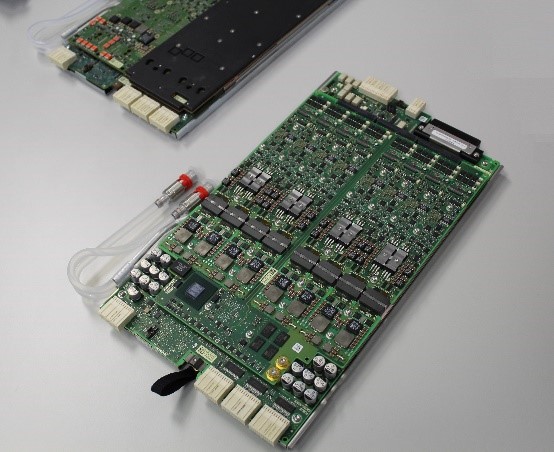
The parallel test technique is enabled by instruments such as the V93000 Wave Scale RF (WSRF) card, which offers test-processor-based synchronization and parallel mission-mode test capability. WSRF can simultaneously test multiple transceiver channels in parallel, thereby improving multisite efficiency (MSE) and significantly reducing test time.

The WSRF includes four independent RF subsystems on each card, with 32 truly parallel stimulus and measurement RF ports per card. Each RF subsystem includes an embedded arbitrary waveform generator and digitizer. The WSRF supports 16x multisite test with native ATE resources and includes embedded RF calibration standards.

For less demanding IoT applications, the WSRF scales down to one RF subsystem for use in an A-Class V93000 system. The WSRF can scale down for IoT, enabling it to perform quad-site testing based on one-fourth of a card using just one RF subsystem. At the other end of the spectrum, you may need four WSRF cards to cover the different needs for both sub-6-GHz and mmWave frequencies.

A concept study involving an LTE-A RF transceiver/RF combo device with 802.11ac support and a 3G/4G front-end module showed that the WSRF resulted in test-time improvements of up to 50% as compared with the PSRF, the predecessor to the WSRF.

Figure 1 (not to scale) depicts receive-channel, transmit-channel, and other tests performed serially (top) and the same tests using a mission-mode parallel technique (bottom). Parallel mission-mode test coupled with test-processor-based synchronization can provide a 40% to 60% test-time reduction. Figure 2 provides specific test-time-reduction values for testing parameters such as gain and EVM in single- and quad-site formats, showing MSE and test-time improvement. The results are based on similar setups and sample rates, with the patterns used being the same.

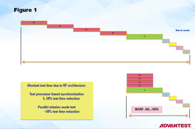
Figure 1. A serial test technique (top) cannot cost-effectively test complex devices, whereas a parallel mission-mode test (bottom) can result in a 50% test-time reduction.


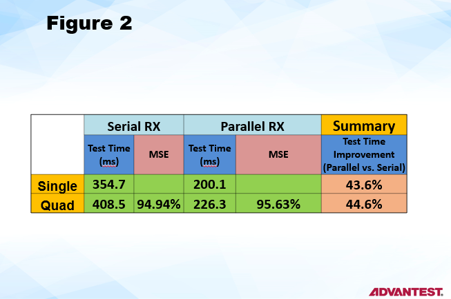
Figure 2. This overview shows multisite efficiencies (MSE) and test-time improvements for parallel vs. serial receiver tests.


Testing 802.11ax

Test of 802.11ax devices offers another example of the benefits of parallel test flow. The successor to 802.11ac, 802.11ax offers an expected fourfold increase in user throughput. Designed to improve overall spectral efficiency in dense deployment scenarios, 802.11ax incorporates multiuser MIMO on the downlink and uplink. It operates in both the 2.4-GHz and 5-GHz ISM bands.

These characteristics impose significant ATE challenges. Multiuser MIMO places more demands on RF/analog resources, resulting in longer test times. ATE RF and baseband instruments (AWGs and digitizers) must accommodate the standard’s 160-MHz bandwidth, and the 1024 QAM modulation scheme demands improved phase noise and linearity.

An eight-site test of an 802.11ax transceiver operating in the 5-GHz band with 4×4 MIMO demonstrates how Wave Scale technology and SmarTest 8 software can test over 4,000 test items, including transmitter, receiver, power-detection, DC, and functional test parameters. The Wave Scale technology includes the Wave Scale RF plus the Wave Scale MX, which includes 16 AWGs, 16 digitizers, 64 PMUs, a hardware sequencer, a real-time signal-processing unit, and a large waveform memory.

Complementing the Wave Scale cards, SmarTest 8 protocol-aware software works directly with user-defined register files and generates a protocol-aware sequence using device-setup APIs with no additional conversion required. The software supports the easy-to-implement flexibleA-Class parallel programming required for concurrent testing. An automated bursting capability works with any type of test, including DC, RF, and digital, and runs as fast as tests based on flat patterns, eliminating the need for manual test-time-reduction efforts, thereby providing an early throughput advantage.

In the 802.11ax example, the Wave Scale instruments powered by SmarTest 8 can test four transmitters concurrently in about 23 ms, vs. 80 ms for a serial-measurement approach, resulting in a test-time reduction of about 70%.

Moving to 5G

5G chips are appearing on the market and can be expected to find their way into 5G handsets and infrastructure equipment in the coming months as 5G deployments roll out. Such devices will increasingly need to rely on parallel test flows to handle the complexities of 5G while continuing to provide backwards compatibility with 3G and 4G technologies, and as they continue to support WLAN, GPS, ZigBee, Bluetooth, and various IoT connectivity applications.

With respect to 5G, new smartphones and other devices will achieve high peak speeds, and 5G will rely heavily on eMBB (enhanced mobile broadband). eMBB will provide not only improved data rates but also broadband everywhere, including in vehicles extending to high-speed trains. Coupled with carrier aggregation, eMBB provides a further example of the benefit for having a parallel test flow that goes hand in hand with test-time reduction and lower COT.

The Wave Scale cards, available now, stand ready to help customers keep pace with the parallel test demands of current and next-generation semiconductor devices.

Read More

Posted in Uncategorized

VOICE 2018 Sets Records with Highest Number of Abstract Submissions from 13 Countries

Advantest’s VOICE 2018 Developer Conference returned to host cities of San Diego, CA, on May 15-16 and Hsinchu, Taiwan, on May 23, where successful VOICE events were held in 2016. The 2018 conference again set records, receiving 177 paper abstract submissions representing contributions from 13 countries. In addition to over 90 technical sessions, VOICE featured Partners’ Expos, highly rated keynote speakers, 25 technology kiosks, and multiple networking opportunities. Altogether, 565 people attended the events, greater than 60 percent of whom represented Advantest customers and partners.

The San Diego event registered 276 attendees, the most of any U.S. VOICE Conference, and included 66 technical presentations, while the Taiwan conference featured 25 papers. Greater than 50 percent of the total papers across both locations were either written or co-authored by customers from 27 companies. The papers were reviewed by a technical committee that included 30 Advantest customers from 14 companies.

With expanded in-app voting capabilities, attendees selected the best technical presentations and, for the first time, the best technology kiosk. At the U.S. event, Jonvyn Wongso from Microchip won best presentation for his paper “Port Scale RF with CTH: Sixteen Sites RF Testing of ZigBee Devices for an IoT Application.”  Ira Leventhal of Advantest was recognized for his kiosk, “Cost-Efficient and Smart System-Level Test for LTE/Cat-M/NB-IoT Devices.”

In Taiwan, Jeff Chen from Qualcomm accepted the best presentation award for his paper “Optimized Probe Tip Life Cycle at Wafer Probing by a New On-Demand Clean Methodology.” Advantest’s Kevin Fan won an award for his kiosk, “FVI16: Next-Generation Floating Power VI for the V93000 — An Instrument Introduction.”

Read More