Pages Menu
Categories Menu

Posted in Upcoming Events

Advantest Opens VOICE 2020 Registration and Announces Keynote Speaker for Scottsdale Event

Arizona Program to Feature Keynote by Social Robotics Expert, Dr. Kate Darling, and Evening Event with Performance by Violinist, Gabi Holzwarth

The Advantest VOICE 2020 Developer Conference will return to two popular locations – Scottsdale, Arizona on May 12-13 and Shanghai, China on May 22 – with the tagline “Your Voice. Your Vision. Our Value.” The learning and networking opportunities offered at VOICE through technical sessions, kiosk showcases, keynote speeches, partners’ expositions and social events will expand in 2020 to include a follow-up day of workshops on May 14 in Scottsdale. 

Online registration opens Wednesday, December 18 with discounted tickets offered for the Scottsdale event through March 27.

In addition to the early registration discount, group discounts are available to attend VOICE 2020; email mktgcomms@advantest.com for details. Those interested in attending the Shanghai event should email mktgcomms@advantest.com for registration information.

VOICE U.S. 2020 Highlights 

On May 12 in Scottsdale, the VOICE program will begin with a keynote speech by research specialist Dr. Kate Darling, a leading expert in robot ethics. Dr. Darling explores the emotional connection between people and life-like machines, seeking to influence technology design and policy direction. Named one of the “Women in Robotics You Need to Know About” by Robohub, she currently investigates social robotics and conducts experimental studies on human-robot interaction at the Massachusetts Institute of Technology (MIT) Media Lab. 

Dr. Kate Darling

That night, VOICE will host an evening event at G Collection, a rare and unique venue focused on showcasing classic European automobiles. The event, to which all registered attendees are invited, will feature the music of classically trained violinist Gabi Holzwarth, and the automobile collection of Scott Gauthier, an internationally acclaimed jewelry designer and car collector. Guest tickets are available for purchase by registered VOICE attendees.

Hotel Reservations 

Registered Scottsdale attendees are encouraged to make their hotel reservations at the Omni Scottsdale Resort & Spa at Montelucia before the discount ends on April 10. For additional hotel information and to make reservations, visit the VOICE website.

Sponsorship

A limited number of opportunities are available in both locations for companies interested in sponsoring VOICE 2020. Contact Amy Gold at amy.gold@advantest.com to learn more.

VOICE 2020 Quick Links

Registration

Workshop Day

Keynotes

Sponsorships

Hotel Reservations

Evening Event

Questions: mktgcomms@advantest.com


Did you enjoy this article? Subscribe to GOSEMI AND BEYOND

Read More

Posted in Featured Products

Advantest’s New Modules and Test Head Extend the T2000 Platform’s Performance in Evaluating Automotive SoC Devices

Advantest Corporation has expanded the range of its T2000 platform with the launch of two new modules and a test head designed specifically for high-volume testing of devices used in automotive applications.  The new equipment is designed to enhance test coverage, enable higher parallelism and reduce the cost of test for system-on-chip (SoC) devices used in automobiles, a market segment that is projected to have a 9.6 percent compound annual growth rate from 2019 to 2022.

Semiconductor content in automobiles is increasing rapidly as ICs are becoming integral in everything from powertrains and infotainment systems to ADAS (advanced driver-assistance systems) and on-board safety features.   To reach their market potential, automotive SoCs require high-performance, cost-efficient test solutions.

The new RND520 test head has 52 slots, providing the highest pin count available with Advantest’s direct-dock testing option. As a member of the HIFIX (high-fidelity tester access fixture) product line, the new test head supports massively parallel wafer-sort testing.  It covers an area 40 percent larger than its predecessor while using center-clamp technology to ensure stable contact during wafer sorting. In addition, the test head can operate over an extended temperature range up to 175° C.

The enhanced 2GDME digital module leverages 256 channels to test a wide range of SoC devices used in automotive electronics including MCUs, APUs, ASICs and FPGAs operating at speeds up to two gigabits per second (Gbps). It features a dedicated high-performance parametric measurement unit (HPMU) for every 32 I/O channels, giving the unit an expanded current capacity up to 60 milliamperes (mA) for every I/O channel. The module also supports high-voltage applications by enabling electrical stress testing and arbitrary waveform generator (AWG) and digitizer (DGT) functions valuable for characterization purposes.

The new 96-channel DPS192A device power supply facilitates highly parallel testing of automotive SoCs with high pin counts.  This versatile module has a voltage range of -2.0 volts to +9.0 volts and a current range up to 3 amperes. The unit’s capabilities include enhanced slew-rate control as well as a trace function to evaluate power integrity, an averaging function that improves sampling rates for measuring supply currents and a continuous sampling function that enables a new test methodology for IDD spectrum measurement.

The highly flexible T2000 test platform is ideally suited for evaluating SoC devices and other ICs fabricated with small-lot, high-mix manufacturing methods.  The system enables users to respond rapidly to shifting market needs with minimal capital investment while also helping to reduce development times for new designs.


DPS192A

RND520


Did you enjoy this article? Subscribe to GOSEMI AND BEYOND

Read More

Posted in Q&A

Q&A Interview with Scott West – Expanding SSD Test Capabilities for Extreme Temperatures

Advantest has found great success with its test solutions aimed at the solid-state drive (SSD) market. In this issue of GO SEMI & Beyond, Scott West, Product Marketing Manager for System-Level Test, provides some background on how the company began to address this market, and shares details on its latest SSD offering, the MPT3000ARC, for validation testing to accommodate extreme thermal standards. 

Q: What was the catalyst for developing this latest addition to the MPT3000 family?

A: Let me briefly recap the MPT3000’s evolution. After spending several years on product research and development, we launched the SSD platform in 2014, signaling a branching out for Advantest from chip test to system-level test. While chips are a single unit, manufactured all at once, with everything controlled by the chipmaker, SSD drives are themselves systems. They’re modules that contain a great deal of flash memory, a controller, controller circuitry, protection capacitors, and other components, which adds further complexities from a test standpoint.

Our focus from the start has been to test SSDs through a protocol interface, including the three primary SSD protocols: SATA [Serial ATA], SAS [Serial Attached SCSI] and PCIe [PCI Express]. All products in the platform test all of these protocols, including PCIe Gen 4, the latest version of PCIe, which is about twice the speed of Gen 3. However, with the ARC system (see Figure 1), we’re expanding in a different direction – we’re looking not just at all SSD protocols, but at all test insertions.

Q: How does this differ from the other MPT3000 products?

A: Each product in the platform has a slightly different, and specific, purpose. The MPT3000EV2 (the second generation of the 3000ENV) is a large-chamber system for reliability demonstration testing (RDT), which is focused on the test design. This involves constant hot and cold temperature cycling of several hundred drives over many months. For example, there is one project we are working on that requires more than six months of constant temperature cycling and testing.

The MPT3000HVM is a rack system designed for production test. It tests each individual drive during high-volume manufacturing to make sure it’s good. It requires not months but several hours, under hot conditions only, with a large amount of power pushed through, to validate that each drive works as expected. It can test quickly because of the rack design – you can put in one drive and immediately begin testing while you’re loading more.

The ARC system addresses a couple of key parameters that the other systems in the family don’t with respect test insertions. The first is extreme temperature range. The standard is referred to as automotive range (-40°C to +105°C), which is where the product name is derived from – ARC stands for Automotive Range Chamber. But automotive is only one application; the standard is also used in aerospace, defense and other ruggedized applications that require extreme temperature range.

The second parameter is high-volume production cold-temperature test. The new chamber was designed to be able to accommodate this type of testing in the production environment, for which the EV2 is not as well suited as it is optimized for very test times. In the enterprise, cold temperature – down to as low as -40°C – is often required for production test. The MPT3000ARC can test up to 128 PCIe Gen 4 DUTs in parallel. Because you have to load the entire chamber at once at ambient temperature, it doesn’t make sense to make it too big, as the ergonomic range needs to be production friendly.

Q: Do all the MPT3000 products have the same pin electronics?

A: Yes, all the systems are compatible with respect to the software and firmware, and all electronics that go to the DUT come from the same test electronics boards. The systems feature up to 22.5G electronics with tester-per-DUT architecture.

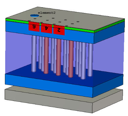
However, the ARC system interface boards, which are designed for the system’s thermal interface, are different from those for the HVM. In the ARC chamber, the chamber is turned on its side, with up to four primitives inserted vertically instead of horizontally (see Figures 2 and 3). This creates a totally closed system that allows air to circulate from right to left inside the chamber, whereas the HVM rack-based system pulls air from the room and then blows it to the back of the system and out into the room. The ARC chamber also features a pocket door designed to accommodate the ergonomic requirements of manual loading and to be automation friendly as well

Q: What are some other key features of the MPT3000ARC?

A: As I mentioned earlier, the system has the ability to test up to 128 DUTs of 50W each. The primary compressor stage has a water-cooled condenser that transfers the energy generated by the chamber load to the test floor’s water-cooling system. This construction helps regulate chamber temperature to ensure consistency. The system has two programmable power supplies for PCIe DUT, targeting high-power enterprise SSDs, and performs current and voltage measurement with high accuracy.

We introduced the MPT3000ARC at the Flash Memory Summit in August 2019, where it was very well received, and the system has shipped to the first customer. We look forward to sharing further successes and advancements in the future.

FIGURES

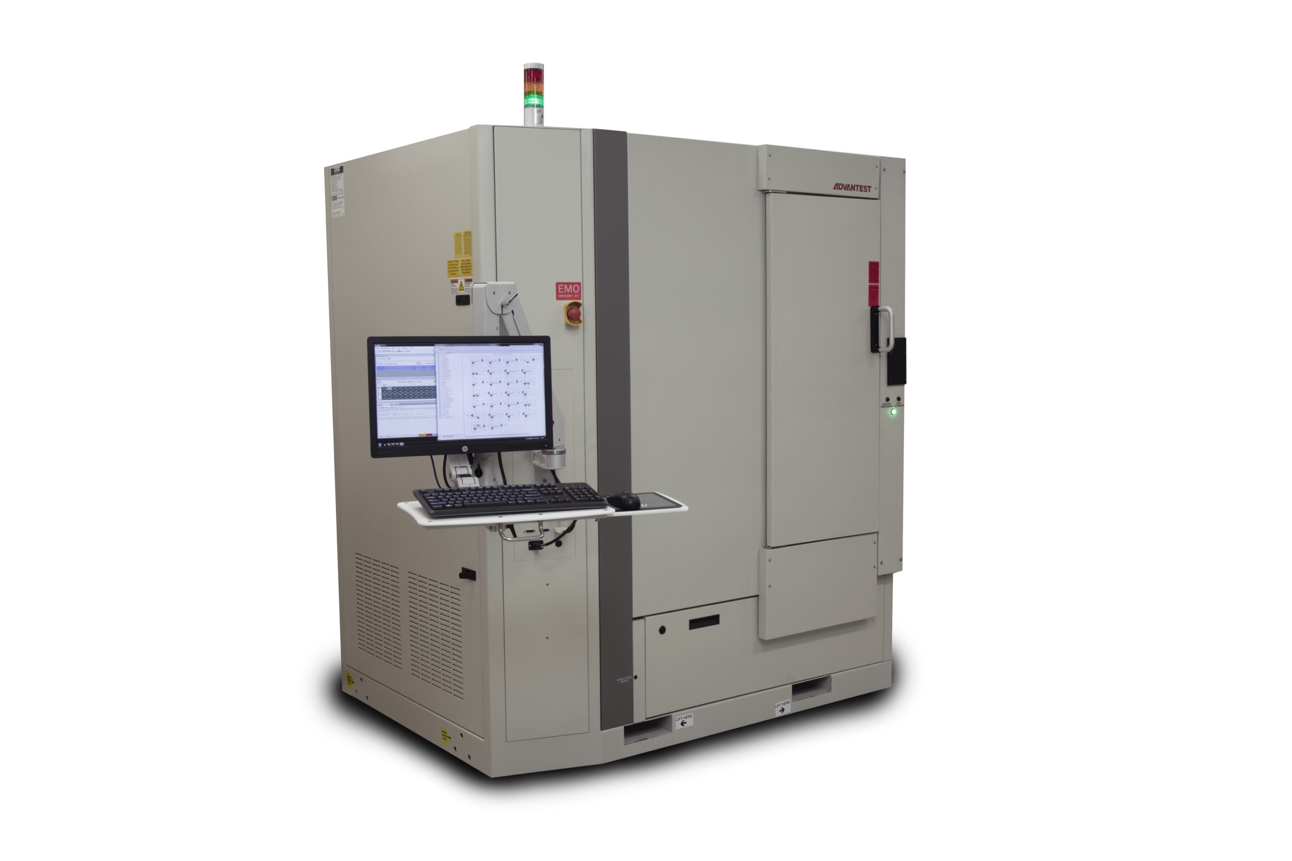
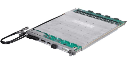
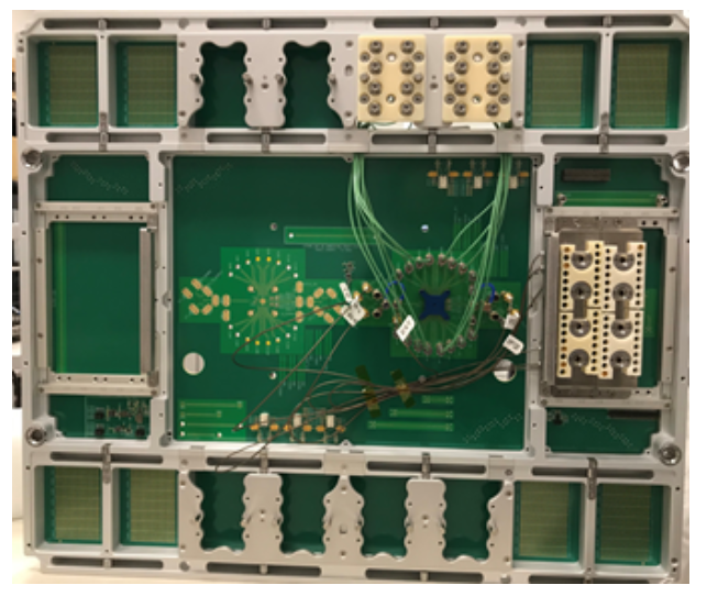
Figure 1. The MPT2000ARC is the latest addition to the MPT3000 family of SSD testers, and tests devices to extreme temperatures.

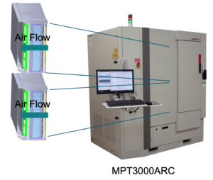
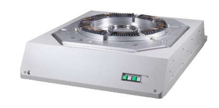
Figure 2. The chamber for the MPT3000ARC is oriented vertically to allow a fully closed system with right-to-left air flow. The primitives are stacked 2×2, back to front. 

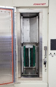
Figure 3. This view inside the ARC chamber shows the positioning of one of the lower primitives in a 64-DUT system.


Did you enjoy this article? Subscribe to GOSEMI AND BEYOND

Read More

Posted in Top Stories

High-Speed I/O Testing with the Power of Two

By Dave Armstrong, Director of Business Development, Advantest America, Inc.

As the internet backbone speed continues to spiral upwards, the interface speeds to the devices making up the cloud also continue to scale up. As many of these interface, server and artificial intelligence (AI) devices move both to 112Gbps data rates and multi-chip heterogeneous integrations, the industry is facing an increased need for at-speed testing in order to confirm truly known-good devices (KGDs).  Until now, an elegant, efficient ATE-based solution for conducting these tests hasn’t been available.

In 2018, Advantest and MultiLane, Inc., a leading supplier of high-speed I/O (HSIO) test instruments, began to explore partnering together to provide a single-platform solution leveraging the best capabilities and qualities of both companies. A fast-growing company founded in 2007, MultiLane is based in Lebanon, where CEO and industry veteran Fadi Daou is committed to expanding the tech industry. With more 200 products and over 500 customers, MultiLane’s product and technology portfolio, as well its corporate culture, are highly complementary to Advantest’s.

The concept of the joint solution is straightforward: existing MultiLane instruments are ported to a form factor compatible with Advantest’s V93000 test head extension frame, as illustrated in Figure 1. As the figure shows, the combined solution consists of an Advantest V93000 tester and twinning test head extension from Advantest, to which MultiLane adds power, cooling and a backplane to create the HSIO card cage. MultiLane then takes existing off-the-shelf instruments and re-lays them out for inclusion in the card cage, which sits on top of the V93000 test head. The use of existing instruments is a key aspect because it contributes to lower cost of test while delivering an already proven capability – just in an ATE environment.

Figure 1. The basic components of the Advantest-MultiLane solution combine to create a unique test offering.

Delving down further into the specifics, Figure 2 illustrates the build-up of the solution. On the bottom is a family board – one of two DUT boards in the build-up – which the customer can typically purchase once and reuse for a variety of testing needs. This bottom board routes the V93000 signals being used to the pogo-block segments located in the HSIO card cage just above, which are then routed to the twinning DUT board at the top of the stack. Multiple MultiLane backplane cassettes sit just underneath the DUT board and device socket, enabling the shortest possible interconnect lead length via high-performance coaxial cabling. The number of cassettes is expandable to include as many as 32 digital storage oscilloscope (DSOs) or 32 bit-error-rate tester (BERT) channels.

Figure 2. The photo at left shows the view from the top of the HSIO card cage with the twinning DUT board and MultiLane instruments removed. 

The setup is designed to be highly configurable. High-speed signals are routed from blind-mate wide-bandwidth connectors to the twinning DUT board mounted connectors adjacent to the DUT. These connectors may be either on the top or on the bottom of the twinning DUT board to provide an optimal signal-integrity solution. Putting the connections on the top of the DUT board allows for direct connection to device signals without the need for routing through vias. For probing, the probe is typically installed on top of the DUT board, with the wide-band connections made on the bottom.  Moving the connectors to the bottom allows the probe to be the only thing extending from the top of the DUT board, as required in a wafer-probe environment.

Another configurable aspect of this solution-set is how bias-tees and splitters are utilized. While very wideband components, these circuits always cause some signal attenuation and distortion. Some users prefer to maximize the signal swing and integrity by not including these circuits in the path. Other users have plenty of amplitude and want the added testability afforded by these components to perform DC tests and/or feed low-frequency scan signal through their HSIO. The flexibility of this approach supports both solutions and allows users to change between them on a part-by-part basis.

Multiple instruments broaden capabilities

MultiLane presently has three pluggable instruments available to coordinate with the V93000 and HSIO card cage. The first can accommodate 58Gbps four-level pulse amplitude modulation (PAM4), while the second is twice the frequency at 112Gbps – the “new normal” data rate. The third is a full, four-channel 50GHz bandwidth sampling oscilloscope, integrated into the solution at a cost far lower than that of a standalone scope, with the same capabilities.  

Figure 3. MultiLane instruments are packaged in cassettes for insertion into the HSIO card cage.   

To ensure the platform solution meets customers’ needs and complementary roadmaps, the MultiLane software and tools are tightly integrated with the V93000. MultiLane eye diagrams and scope plots can be brought up in standard V93000 SmarTest tools (see samples in Figure 4). The scope can also analyze results in the frequency domain to provide a distortion analysis, as is typically done on a vector network analyzer (VNA).   


Figure 4a. MultiLane BERT output waveforms shown on the V93000.


Figure 4b. MultiLane DSO measurements shown on the V93000.

Conserving tester resources

A noteworthy capability of the solution is that the entire HSIO card cage and MultiLane instrument assembly can be used on the bench together with the V93000 DUT boards – i.e., they can run independent of the tester. In some cases, it may be possible to add a simple bench power supply and a PC interface to allow some long-running measurements to be made without the V93000. 

Returning the HSIO card cage on the tester, a local PC can also be used to talk to the MultiLane instruments via the internet. For example, the tester’s SmarTest program can be sequenced to an area of interest and pause, at which point a PC can interact with the MultiLane hardware to interactively explore and analyze the results – much like a scope would be used in the old days, only without the need for probing the fine-geometry wide-bandwidth interfaces. This unique capability both improves the utilization of the HSIO Instruments and allows the user’s offline experience, with the device and instruments to be leveraged into the ATE environment thereby improving efficiencies in both locations.   

Bringing it all together

Developing leading-edge test solutions in the 112Gbps area requires close collaboration and involvement with experienced high-speed I/O experts. Working together with our mutual customers, Advantest and MultiLane can leverage the strengths of both companies to help ensure success and provide the full benefits of this truly unique ATE-meets-HSIO test-platform solution.


Did you enjoy this article? Subscribe to GOSEMI AND BEYOND

Read More

Posted in Featured Products

Evaluating a spring probe card solution for 5G WLCSP

By Krzysztof Dabrowiecki, Feinmetall GmbH, Thomas Gneiting AdMOS Gmb], Jose Moreira Advantest

With the deployment of the wireless 5G standard and its support for mmWave frequencies that allow gigabits-per-second data rates on the consumer market, the semiconductor industry needs reliable and low-cost test solutions. The 5G standard allows mmWave range frequencies from 24GHz to 28GHz—to frequencies as high as 44GHz, and possibly even higher.  To achieve these frequencies requires reliable, highly efficient, cost-effective chip packaging technology. 

From that point of view, wafer-level chip-scale packaging (WLCSP) offers one of the most compact package footprints, providing a high level of functionality, and a frequency range with low resistance and inductance path. Despite having a good thermal performance with a finer pitch interconnection to the printed circuit board (PCB), WLCSP is resilient to extreme variations in stress, drop, and vibration. At the wafer test level, WLCSP technology requires a good and consistent contact resistance, a relatively high contact force with short probes, and above all, an effective online cleaning together with easy onsite repair [1]. With respect to those electromechanical wafer test requirements and with added value such as a frequency performance higher than 28GHz, or a high current capability, the spring pin probe card technology is always a favorite on the test floor on account of its cost and versatility and worthwhile to evaluate for high frequency 5G mmWave applications [2-4].

To define the best possible probe card structure, detailed electromagnetic simulations and analyses are required. RF engineers have several modeling approaches available for this type of simulation, such as a lumped element model (SPICE), distributed element model, or 3D electromagnetic (EM) models. For this study, it was decided to utilize CST Studio Suite 3D EM simulation software.  It allows us to build and analyze an exact and detailed 3D-model of the probe card. A probe card acts as an interconnector on the signal transmission path between the wafer chip and automated test equipment (ATE). Therefore, it is vital to keep in mind that, besides the probe card, there are other challenges with respect to ATE and the PCB side.

On the ATE side, mmWave frequencies already present significant implementation challenges, including the measurement instrumentation and interconnect to the ATE device under test (DUT) test fixture PCB.

Figure 1

Figure 1 shows a picture of the bottom of an ATE mmWave test fixture, where it is possible to observe the blind mating connectors to the ATE system and the coaxial cables. They are connected to coaxial connectors, very close to the socket. The use of coaxial cables in the test fixture is essential because a coaxial cable is significantly less lossy than any PCB signal trace. The PCB test fixture challenges, however, are not the main subject of this paper.

The system assembly and modeling (SAM) framework was used to investigate and optimize a signal path. It consists of multiple individual components, such as wafer bump, probe head, and PCB. These are described by relevant physical quantities such as field magnitudes or s-parameters.  This paper is trying to find an answer and explore three objectives: 1) the impact of different materials and probe head designs on the mmWave performance, 2) analysis of s-parameters and crosstalk, and 3) the probe head design optimization to improve them. Crosstalk is also an important parameter that is taken into account. The presented analysis results reveal the impact of different structure probe head elements on the s-parameter results.

Simulation model

Figure 2

Figure 2 shows an example of what mmWave RF peripheral ports (AN1, AN2) might look like on a 5G DUT. The diagonal bump pitch is 0.4mm, with a bump height of 100mm. The distance, in a row, between RF bumps is 0.566mm. Initially, a spring pin was chosen with uncompressed length L=3.7mm, at working mode L1=3.5mm.  The PCB thickness was 3.8mm and used a hybrid stack-up of the FR4 and Tachyon 100G for dielectric material. The matched trace lengths were designed at 38.8mm. Because of the symmetrical PCB traces layout, the simulation was performed for the critical traces only and one-quarter of the PCB. The RF 3D model analysis includes the wafer solder bump, probe head, and contact with the PCB, in which the traces are included up to the connector locations. 

Figure 3

Figure 3 illustrates a quarter of the probe card model and trace topology.

Figure 4

Figure 4 shows a model of a probe head in contact with the wafer at the bottom and the PCB at the top. The probe head is a 2-layer structure comprising guiding plates and fillers between the plates. The filler layers are the additional materials added between the guiding plates with various dielectric constants and loss tangent. The double plunger spring pins are inserted into drilled holes in the guiding plates and fillers. The pin plunger protrusions at the working mode are formed with a uniform air gap of 0.1mm between the head and the PCB, and 0.25mm between the head and wafer. The created 3D simulation model allows quick verification of results to identify appropriate material properties and geometry before building a test probe card.

Initial simulation results

It is well-known that any impedance mismatch in the signal path will have an impact on the return loss and in that way, degrade the measurement path performance. Therefore, impedance is a crucial parameter to be checked and controlled. In the PCB industry, the common impedance specification is in the range of 50 +/-10% Ohm for a single ended signal. But 5% is possible in certain cases, though at a very high cost.

Figure 5

Figure 5 shows the simulated time domain reflectometry (TDR) plot for the model with various filler materials wit a time rise of 29.2ps (for 30GHz). The dashed lines indicate the maximum and minimum impedance tolerances. In the figure, it can be noticed that the air gap between the guiding plates causes an impedance discontinuity that peaks at

70 Ohms. The material option 1 shows a drop in the impedance discontinuity peak at 41 Ohm. The material B options 2 and 3 significantly reduce the impedance discontinuity to an acceptable range. As a consequence of material B air and option 1, the insertion loss and return loss had a limited frequency bandwidth, as shown in Figure 6. In this case, the dashed lines reveal acceptable limits of -1dB for insertion loss, and -10dB for return loss.

To read full article please visit Chip Scale Review December 2019 issue, page 14:  http://fbs.advantageinc.com/chipscale/nov-dec_2019/52/


Did you enjoy this article? Subscribe to GOSEMI AND BEYOND

Read More