Pages Menu
Categories Menu

Posted in Featured

Advantest’s myAdvantest Online Portal Provides 24/7 Access to Digital Products and Web-Based Services

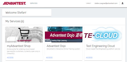
Advantest has introduced a new online portal enabling customers to place orders and get instant delivery of Advantest’s cloud-based services and software products, making these items available on demand, anytime and anywhere.  Users can access the myAdvantest portal from any internet-connected device without having to install an app or software program.

One of the portal’s initially available services is interactive online training.  Dojo™, the Advantest Online Training System, is a cloud-based eLearning service.  In addition to offering self-paced, interactive multimedia courses, Dojo also offers unlimited access to a virtual SmarTest Software Playground environment for practicing and executing lab simulation tests as well as live interactive sessions with Advantest experts to discuss, practice and demonstrate SmarTest’s capabilities on real V93000 testers.  This online training leverages the most modern eLearning methodologies to supplement traditional classroom training sessions and offer the unmatched flexibility of web-based courses.

In addition, cloud-based test engineering is available for the first time with the innovative Test Engineering Cloud (TE-Cloud™), a Platform-as-a-Service (PaaS) solution that is accessible exclusively through myAdvantest.  With this one-stop test engineering platform, customers can utilize a complete test development environment online including an integrated set of software tools for test program development, standard test IP libraries and a suite of self-help tools such as customer forums, documentation and training.  Moreover, online interaction with Advantest technical support and application engineers is available on demand to help with tasks such as remote debugging of test programs. TE-Cloud’s pre-installed software bundles are scalable and offered as flexible subscription options.  

The myAdvantest portal makes it easy for Advantest’s customers to educate their personnel and develop test programs while also reducing their investments of time and capital to bring new device designs to market resources.  This launch represents a new era in how Advantest serves their global customer base.

Your Digital Gateway for all Advantest Cloud Services: https://myAdvantest.com


Read More

Posted in Upcoming Events

Advantest Extends its Global Reach at the First-Ever Virtual SEMICON West 2020

Contributed by Jess Nguyen

For the first time, the SEMICON West 2020 trade show commenced on July 20-23, 2020 as a full-on virtual event. To stay connected with its customers, Advantest returned as a Gold Sponsor and exhibited a virtual booth featuring graphics and videos of its latest end-to-end IC test solutions for cutting-edge applications such as 5G and artificial intelligence (AI).

Drawing nearly 480 booth visitors, Advantest showcased its novel V93000 Wave Scale™ RF8 card for testing 5G-NR transceivers and connectivity-ICs operating at frequencies up to 8GHz, along with its new myAdvantest online portal, a platform providing 24/7 access to web-based services including the new Test Engineering Cloud (TE-Cloud™).  Other displays included comprehensive test cell solutions for AI and high-performance computing (HPC) applications using the V93000, T5800 series, or T5503 testers; Advantest Test Solutions (ATS) and the MPT3000 series test platform for integrated system-level test (SLT); and an array of software tools and services for enhancing test performance. 

Advantest was also a sponsor of the Test Vision Symposium and presented live during two of the sessions. Adrian Kwan, senior business development manager, presented on “5G NR Semiconductor Test Challenges”, and Zhi-Jun Xue, consulting manager, presented on “Test Cell Management for Enabling SMART Manufacturing”. For the SMART Mobility Pavilion, Masashi Nagai, senior executive director, presented “Driving for Perfection: Finding the Optimum Test Solution for Next-Generation Automotive ICs” which was made available for on-demand viewing. 

To support the next generation of industry professionals, Advantest sponsored and participated in the SMART Workforce Pavilion and SEMI’s High-Tech U program for the third consecutive year. This career development program was designed to inspire and assist college-level students with their job search during these uncertain times. Advantest contributed a video featuring anecdotal tips for navigating a virtual job search environment.

Joining in on the first virtual SEMICON West was a valuable, unique experience for Advantest. The SEMI virtual trade show served numerous industries including the semiconductor, sensors, MEMS, photonics and the automotive sector. With 67 different countries represented at the event, it presented us with an opportunity to demonstrate both our commitment to the semiconductor industry and our ability to continuously adapt to new ways of collaborating and networking with our global customers, partners and employees. Our “yes” attitude, which is a component of Advantest’s core values, allows us to take the bold steps needed to be at the forefront of innovative technologies and leadership.

Read More

Posted in Featured Products

Advantest’s New TS9001 Time Domain Reflectometry (TDR) System Employs Terahertz Technology to Provide High Resolution Analysis of Circuit Faults

Advantest Corporation announced that it has initiated sales of its new TS9001 TDR System. The new system fully utilizes the company’s unique terahertz technology to enable non-destructive and high-resolution analysis on circuit faults in advanced semiconductor packages, such as flip chip BGAs, wafer level packages, and 2.5D/3D ICs. 

The TS9001 TDR System provides semiconductor manufacturers with flexible solutions for addressing a variety of failure analysis requirements. By establishing a low-cost failure analysis environment and enabling connections to high-frequency probing systems already in use by customers. TS9001 offers customers one of the shortest measurement times on the market. 

Advantest’s leading-edge semiconductor test technology and terahertz failure analysis technology supports the development of innovative semiconductor supply chains, while enhancing the customers’ quality control. 

Background

As semiconductor packages (hereafter, devices) grow smaller and more highly integrated, the ability to locate failures with non-destructive, high-resolution technology is increasing in importance. Providing access to the industry’s most advanced failure analysis environment is critical to being able to address the wide variety of failure analysis issues that are present in these complex devices. To meet these requirements, Advantest developed the TS9001 TDR System, which enables customers to direct-connect their high-frequency probing systems, to obtain high-speed, high-resolution measurement. 

Key Features

  • High-speed and high-resolution measurement

The TS9001 TDR system, which utilizes an ultra-short pulse signal processing technology,  achieves higher distance-to-fault resolution of 5 μm and precise fault location identification with the industry’s fastest class measurement time of 30 sec (Number of integration: 1024, 1/10 shorter than our conventional products). This is the same proven technology used in our ground-breaking terahertz analysis systems.

  • Versatile connectivity for high-frequency probing systems

TS9001 can be configured with a high-frequency probing system owned or selected by the customer. It offers flexible solutions according to the device forms or fault analysis environments. 

(1) Failure analysis of devices with micro bump

By connecting the TS9001 to a high-frequency probing system along with a high-resolution microscope, failure analysis of devices with micro bump of minimum diameter 50 μm is possible. 

(2) Temperature control function

Failure analysis of devices kept in low/high temperatures is also possible, if the system is connected to a high-frequency probing system with a thermal-system function.  

(*) TDR (Time Domain Reflectometry) is widely used to locate circuit failures. Input pulsed signals are reflected at circuit faults inside the device. Time domain analysis of the reflected waveform allows users to determine the fault location and failure mode (open or short) by waveform comparison between good device and failed device. The peaks appearing only in the failed device are analyzed to identify them. 

For more information on this system, visit our Website. 

URL: https://www.advantest.com/products/terahertz-spectroscopic-imaging-systems/tdr-option

Read More

Posted in Featured Products

New Memory Tester Integrates Burn-In and Core Testing for 5G Product Development

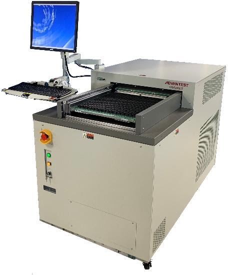
Advantest has added to its H5600 family of memory testers by introducing the new, highly versatile H5620ES engineering test system, designed for both high-speed burn-in and core testing of today’s DDR4, next-generation DDR5, and low-power, double-data-rate (LPDDR) devices in laboratory environments.  By streamlining the number of accessories and reducing the time required between burn-in and core testing, the new H5620ES shrinks the cost of test for evaluating advanced memory devices used throughout 5G applications.  The new system ably addresses all barriers to cost-efficient development and qualification of the newest data-storage ICs that are in high demand for the rapidly growing 5G market.

Like its sister system, the H5620 production unit introduced in March of this year, the new tester delivers high productivity by parallel testing both DDR4 and DDR5 memories. It can accommodate memory ICs with 100-MHz frequencies and 200-Mbps data rates. 

The engineering system is optimized for ease of use in product development, enhancing testing efficiency in the lab prior to production.  Its compact design saves space and enables mobility in laboratory environments while its open-top architecture makes it easy to perform pick-and-place operations without removing the device interface board (DIB).

The H5620ES runs on the same FutureSuite™ operating system as the H5620 production unit, enabling testing with the same waveform.  It also allows pre-testing routines such as contact checking to be conducted on the H5620ES system before transfer to the H5620 tester, thereby reducing cycle times in production.

Read More

Posted in Q&A

Q&A Interview: Moving Test to the Fast Lane

By: GO SEMI & BEYOND Staff

In this issue, our Q&A interview subject is Steve Pateras, Senior Director of Test Marketing for Synopsys. Steve provides a look at a new test capability, jointly developed by Synopsys and Advantest, that leverages high-speed communication interfaces such as USB and PCIexpress to improve test throughput. (NOTE: This piece was originally intended to serve as a preview of Steve’s VOICE 2020 keynote address; although canceled this year, the conference will return in 2021, as will Steve.)

Q: What was the catalyst for developing this approach?

A: The industry is always looking for new ways to improve test throughput, in order to reduce test times and costs. As chip designs get larger and larger, you need more test data, so to keep test costs in line, you need to improve bandwidth to get better throughput.

Moore’s Law kept things growing and increasing in complexity over the past several decades, but periodically, fundamental paradigm shifts needed to happen. The first was in the 1980s, when we moved to structural test because chips had become too complex to cover all possible failure modes using functional verification. Looking only at the I/Os related to flip-flop scan chains, rather than every functional I/O, became the new norm, and this worked well for a couple of decades.

By 2000, scan alone had become inefficient – the number of scan chains and I/Os to scan kept growing larger and larger, and the sheer volume of data was too massive to store on the tester. This led to the next paradigm shift: compression channel I/O. Data is compressed on the tester, then sent to the chip, where it is decompressed on-the-fly into multiple scan chains. Again, this reduced the number of I/Os and test times to a manageable amount. Another 20 years passed, which brings us to today.

As chip features shrink down to 14nm, then to 7nm and beyond, we’re still seeing exponential growth in the numbers of patterns and pattern test data. We’ve again reached the point where we can’t accommodate the volume – even compressed, there is too much data to be stored, and it takes too long to scan data in and out. It’s time for a new approach.

Q: You’re talking about the next paradigm shift?

A: Exactly. Structural (scan) patterns form the primary test for digital logic – more patterns are required to maintain quality, with larger designs requiring more manufacturing tests, and new process nodes demanding advanced fault tests. At some point, things start to break; how do you achieve the necessary bandwidth when you have limited tester speeds and a limited number of available pins? Figure 1 shows real-time bandwidth limitations – that is, the actual number of gigabits you’d need to test some of the newer, larger devices. Existing approaches can’t accommodate moving from tens to hundreds of gigabits per second, let alone into the terabit range. 
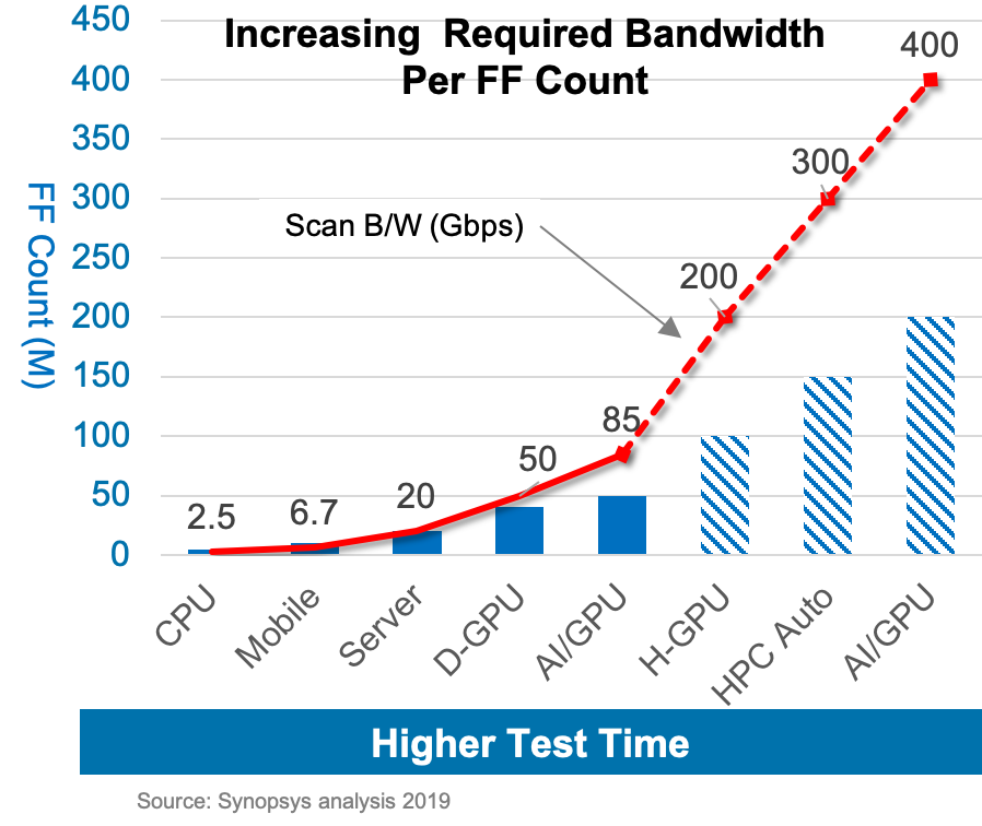
Figure 1. As data volumes increase with device complexity, test times rise sharply.

What we’ve been developing with Advantest is the use of high-speed functional I/O (HSIO) to increase bandwidth. Instead of feeding the compression logic onto the chip via dedicated scan I/O, we’re using very high-speed serial functional interfaces, i.e., USB and PCIexpress, to achieve this. Once the data is entered, we can convert it into the parallel data we need to feed the compression logic. We use these very high-speed serial inputs to get the required bandwidth, and then we parallelize this widely to all the many parallel scan chains on the chip. 

Q: How is the parallelism achieved?

A: Via the on-chip logic that we provide, which works essentially like a transformer. It allows for very large amounts of data coming without the need for dedicated, lower-speed I/Os. We’re essentially reusing the high-speed interfaces that exist on virtually every chip today. Instead of reinventing the wheel and adding more dedicated pins per test, we simply piggyback on top of these interfaces during the test process to send high-speed test data through them [Figure 2].

Reusing these existing high-bandwidth functional interfaces offers three key benefits: it reduces test time; it eliminates the need for dedicated test I/O; and it provides test portability through the product lifecycle. 
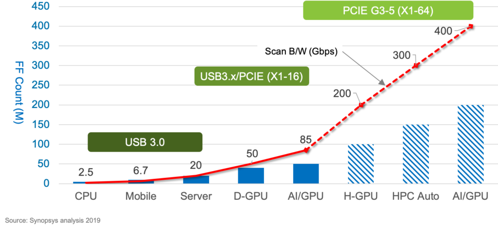
Figure 2. Reusing HSIO protocols improves scan bandwidth, significantly lowering test times.

Q: How long has the new solution been in development, and what does it entail?

A: We’ve been working with Advantest on this new HSIO paradigm for over two years, combining key components from our TestMAX suite of software with Advantest’s V93000 SoC tester. The solution entails three key aspects, summarized in Figure 3:

  1. Packetizing manufacturing test data to accommodate HSIO protocols. Integrated into the V93000, our software [dark green box] takes traditional parallel data from ATPG tools, converts it into high-speed packet data, then depacketizes the data coming back and maps it to known failure descriptions.
  2. Enabling the tester to accommodate this approach [light green box]. Testers themselves need to be able to drive data through these high-speed interfaces, so through this joint effort, Advantest has added new hardware onto the V93000 to provide the HSIO function and ensure their SmarTest software can work with it.
  3. Ensuring the chips can handle this high-speed packet data. We devised a bidirectional HSIO-to-DFT interface controller, which is added to the chip as IP [dark grey box] to actively manage incoming high-speed packet data on one end and receive the parallelized lower-speed test data on the other.
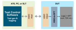
HSIO Test Paradigm Diagram

Figure 3. The new HSIO test paradigm integrates key software, hardware and on-chip functionality.

In addition, our Adaptive Learning Engine (ALE) adds more intelligence to the test process. It allows our software to actively look at failure data coming back from the device and adapt the test to deal with the kind of failures that are being seen on the tester, as well as perform more advanced diagnostics. This can be performed locally on individual testers, as well as on a Big Data level – each tester on the floor can send its results to a centralized analytics engine analyzing results and looking for systematic issues across multiple devices over time. In this way, we can help to greatly improve the test process at the test-floor level.

For more details, real-world examples and updates on this new high-speed functional I/O test paradigm, make plans now to attend Steve’s keynote address at VOICE 2021 in Scottsdale, Ariz.

Read More