Pages Menu
Categories Menu

Posted in Featured Products

Advantest Launches KGD Test Cell for Power Semiconductors

Late last year, Advantest announced an integrated test cell designed to maximize die-level test yields for wide-bandgap (WBG) devices essential to power semiconductors. The Advantest Known Good Die (KGD) Test Cell combines the company’s CREA MT Series power device testers with the new HA1100 die prober. 

Demand for power semiconductors continues to grow with the rapid escalation of electric vehicles (EV) and power infrastructure. WBG devices, particularly silicon carbide (SiC) and gallium nitride (GaN), are essential for the design and manufacture of power semiconductors, enabling them to be smaller, faster, and more efficient than silicon-based devices. However, failure screening of WBG devices is challenging, as the probe card, the chuck, and the devices can be damaged due to the devices operating at very high voltage and current. 

Essentially serving as a one-stop shop for efficient equipment management, the Advantest KGD test cell solution helps reduce customers’ manufacturing costs. CREA’s proprietary probe card interface (PCI) technology can eliminate damage risk. Even if damage issues occur, Advantest will investigate it with the test cell. Customers can minimize the downtime of the test cell. The HA1100 die prober for the CREA MT Series test systems enables assembly of dies in power modules using only passed (KGD) die, ensuring no failed die find their way into the module. This prevents yield loss at module test, thus reducing the loss of final multi-die assembled power modules.


Read More

Posted in Featured Products

Advantest Launches ACS Gemini™ – New Developer Platform for Accelerating ACS RTDI™ Application Development

Last December, Advantest announced the launch of its new software development platform ACS Gemini™, which allows customers to develop, simulate and debug machine learning applications in a virtual environment. The digital twin of ACS RTDI™, ACS Gemini is part of Advantest’s mission to enable customers and partners to utilize data analytics in developing artificial intelligence (AI) and machine learning (ML) solutions for semiconductor testing. 

In recent years, manufacturing costs for semiconductors have increased significantly due to their growing complexity. Analysts at McKinsey & Company predict that implementing AI and ML could lower manufacturing costs by 40%, as many engineers use these technologies to optimize efficiency in manufacturing. 

ACS Gemini improves efficiency by providing customers with a seamlessly integrated experience that optimizes design-to-production proficiency in the virtual ACS RTDI environment. The digital twin software solution is composed of the ACS Software Development Kit, Reference Application Development Model, and Containerized applications publishable to the ACS Container Hub™. These elements enable customers to simulate valuable test results in a virtual production setting. 

ACS Gemini saves customers time and cost in engineering debugging, design vs. production correlation, and cloud deployment of apps—ultimately saving valuable tester time. Overall, the solution accelerates ML application development, simulates testing results, and shortens time-to-deployment of ML applications on the production test floor. 

Advantest’s ACS RTDI is a real-time data infrastructure platform-as-a-service that securely collects, analyzes, stores and monitors semiconductor test data to empower customers to automate the process of converting insights into actionable test decisions within milliseconds. This helps customers and partners reduce test time, optimize quality and reliability and enhance smart packaging.

Read More

Posted in Q&A

Interview with Oded Olansky, VOICE 2025 Chairperson

Advantest’s VOICE 2025 Developer Conference will take place May 12-14 at the AT&T Conference Center in Austin, Texas. To learn what VOICE 2025 holds in store for attendees, we interviewed this year’s general chairperson, Oded Olansky, WCS RF Products Si Test Architect and WCS Haifa Wireless Test Engineering Manager, Intel.

By GO SEMI & Beyond Staff

Q. With VOICE 2025 taking place in Austin, how will this year’s location impact the event?

A. Austin is significant to the semiconductor industry. Major companies like Tesla, Amazon, AMD, Microsoft, and NXP have a strong presence in the area, with Texas Instruments located nearby in Dallas. This makes Austin a vibrant hub for industry and innovation, which is why we believe it is the perfect location for VOICE 2025. With our venue situated in the bustling heart of the city, we are excited to host VOICE 2025 in Austin and invite our attendees to enjoy the city’s rich culture.

Q. As the VOICE 2025 chair, what do you hope to see, or what do you hope attendees will gain?

A. For me, the VOICE conference has always represented a unique opportunity to explore emerging technologies and innovative testing methodologies, whether through presentations, kiosks, or invaluable networking opportunities with test engineers from diverse companies and countries. I hope that attendees of this year’s conference will experience the same. Personally, I believe that if, upon returning from the conference, I can apply even one new insight or idea successfully in my work, then the conference has been both successful and worthwhile. I encourage the attendees of VOICE 2025 to set a similar goal for themselves.

Q. I heard that there will be an exceptional number of presentations at this year’s event. What presentation topics and industry trends are you most excited about? 

A. Our committee accepted over 100 technical papers this year, with a record line-up of over 130 presenters. These numbers tell us that people are excited about the state of the industry right now and are eager to discuss the latest trends and innovations with their peers. 

I believe we are currently witnessing a transformative revolution in the field of artificial intelligence, particularly in the area of generative AI. This revolution strongly echoes the impact of the Internet revolution, which began around the time I started my career in test engineering. As such, I am particularly eager to see presentations and engage in discussions surrounding this topic, as it promises to reshape the industry in profound ways.

There will also be presentations regarding the new instruments for the V93000 EXA Scale platform that were announced last year, including the DC Scale XHC32 ultra-high-current power supply. Presentations will also feature the new PMUX02 advanced power multiplexer for the V93000, which offers unprecedented capabilities for multi-site testing of power and analog devices, including battery-management systems (BMS), automotive, and power management IC.

Q. What highlights of this year’s event do you recommend attendees not miss?

A. There is plenty to look forward to at VOICE 2025. The conference will kick off on Monday evening with a welcome reception, offering a great opportunity to network with representatives from top semiconductor companies. At the same time, we will host the Technology Kiosk Showcase, featuring exciting displays of cutting-edge innovations that highlight Advantest’s diverse product portfolio.

Tuesday and Wednesday will feature engaging keynotes from semiconductor market analysts and leading professionals. The Partners’ Expo is also open throughout Tuesday and Wednesday, allowing attendees to engage with our technology partners to discuss their latest products and solutions.

Tuesday’s evening event will be hosted at The County Line—a charming lakeside lodge serving classic Texas BBQ and margaritas. The setting provides a relaxed atmosphere that is perfect for mingling with colleagues while enjoying the stunning views of the lake from the venue’s redwood deck. We also have a great lineup of fun Texan-themed activities that everyone can enjoy throughout the evening, including horseshoe tossing and even line dancing lessons. There’s plenty to look forward to, and we invite all attendees to join the fun.

We will wrap up VOICE 2025 on Wednesday afternoon with an awards ceremony honoring the best papers and those receiving honorable mentions. Additionally, we’ll present the Visionary Award, given annually to a customer who has made significant, lasting contributions to VOICE over the years.

Q. Who will be joining us for this year’s keynote addresses?

A. VOICE 2025 will feature three dynamic keynote speakers. 

Our first speaker on Tuesday will be John Yi, a Fellow at AMD. With over 30 years of experience, John currently manages a team of test architects responsible for defining new design-for-test (DFT) methods and test solutions with silicon design and product engineering groups that span a wide spectrum of AMD products. 

Our next two keynotes will be on Wednesday, starting with John Yick, senior director of product and test engineering at Marvell. John leads Marvell’s product and test engineering teams, driving the production of cutting-edge broadband analog devices such as trans-impedance amplifiers and drivers, as well as silicon photonic integrated circuits (PICs). His expertise spans a wide frequency range, from DC to 110 GHz, all the way to light speed.

Roy Meade, TIE executive director of strategic partnerships at the University of Texas, will present our final keynote on Wednesday. Throughout his career, Roy has exhibited exceptional innovation and leadership in the domains of photonics, packaging, and memory technologies. His contributions to these fields are evidenced by over 120 patents granted by the United States Patent and Trademark Office, encompassing photonics, semiconductor manufacturing, and emerging memory technologies.


As a final note, we would like to thank our VOICE 2025 sponsors for making this year’s event possible—in particular, our headline sponsors, ISE Labs, ASE Group and Alliance ATE Consulting Group. The full list of sponsors can be found here.

To learn more about keynotes, papers, and other details related to VOICE 2025, be sure to keep checking the VOICE website. And don’t forget to register here to reserve your spot!

Read More

Posted in Top Stories

The Future of Semiconductors: Trends, Challenges, and Opportunities

This article is adapted with permission from a recent Advantest blog post.

By Keith Schaub, Vice President of Technology and Strategy at Advantest

The semiconductor industry is experiencing a significant transformation driven by technological advancements, market dynamics, and geopolitical factors. In a recent episode of Advantest Talks Semi, Andrea Lati, a leading expert in semiconductor market analysis at TechInsights, provided an in-depth discussion on the forces shaping the industry, key challenges, and the future outlook.

A Market on the Rise

The semiconductor market has performed far better than expected in 2024, with a projected 23% increase in overall sales and a 28% surge in IC sales—the fastest growth in over a decade, according to Lati. This surge marks a robust recovery from the downturn experienced in 2022 and 2023. The market cycle, says Lati, which typically fluctuates every two to three years, suggests that 2025 and 2026 will continue this upward trend.

However, what makes this growth particularly interesting is that it is primarily driven by increased average selling prices (ASPs) rather than unit volume growth. Two major factors contributing to this trend are the recovery of the memory market—specifically DRAM and NAND—and the explosive impact of NVIDIA’s AI-driven demand.

The AI Boom and Market Disparities

AI and high-performance computing (HPC) have become the primary drivers of semiconductor market growth, pushing demand for advanced logic and high-bandwidth memory (HBM). While AI-related semiconductor sales have soared, broader market segments such as PCs, smartphones, and automotive remain in a recovery phase. These sectors still struggle with excess inventory, limiting their growth potential in the near term.

Despite the strong AI-driven upturn, unit volumes for semiconductors are projected to grow by only 2% in 2024, according to Lati. This discrepancy highlights an imbalance in the market, where AI applications drive demand while traditional segments experience slower rebounds.

Geopolitical and Supply Chain Considerations

A major factor influencing the semiconductor industry is the evolving global supply chain. Over the past few years, China has significantly increased its capital expenditures in semiconductor manufacturing, with three Chinese companies ranking among the top 10 CapEx spenders for the first time. In 2023, China accounted for 35% of total wafer fabrication equipment (WFE) spending, and this figure is expected to rise to 45% in 2024, according to Lati.

Government funding also plays a significant role, with approximately $200 billion in semiconductor-related government incentives across the U.S., China, Japan, and Europe. However, this influx of investment raises concerns about potential overcapacity, particularly in trailing-edge technologies, which could lead to supply gluts and increased tariff measures in Western markets.

The Future of Semiconductor Technologies

Looking ahead to 2025, several key trends and technologies will shape the industry’s evolution:

  1. Advanced Packaging and Chiplets: As Moore’s Law slows, semiconductor companies are increasingly turning to advanced packaging solutions such as chiplets and 3D stacking. Chiplet technology enables continued performance improvements at the system level, even as traditional transistor scaling reaches its physical limits.
  2. Silicon Photonics: AI and HPC applications require immense bandwidth and energy efficiency, making silicon photonics an attractive solution for reducing power consumption and latency in data centers.
  3. Expansion of AI Infrastructure: The capital expenditures of major hyper-scalers are projected to exceed $300 billion in 2025, with most of this spending directed toward AI-driven data center expansion.
  4. Automotive Semiconductor Growth: While overall vehicle production remains steady, semiconductor content per vehicle continues to rise due to the proliferation of electric vehicles (EVs) and advanced driver assistance systems (ADAS). By 2029, the automotive IC market is projected to surpass $100 billion.

AI and the Future of Semiconductor Testing

As AI continues to transform semiconductor technology, manufacturers require advanced solutions to handle the increasing complexity of AI-driven chips and real-time data processing. Advantest’s ACS RTDI™ (Real-Time Data Infrastructure) is a key innovation addressing these challenges, providing a robust ecosystem for real-time data collection, processing, and simulation.

Key ACS RTDI™ Recent Advancements:

  • Seamless Integration: Accelerates machine learning (ML) application development with ACS Gemini™ and other tools in the Advantest ecosystem, reducing time-to-market.
  • Cross-Test-Floor Data Streaming: Enables secure, efficient Data Feed-Forward (DFF), allowing data to be streamed seamlessly from one test floor to another.
  • Automated ML Model Deployment: Simplifies the deployment of AI/ML applications in OSAT production environments, with RTDI now available at leading OSATs and foundries.
  • Data-Driven Decision Making During Test: Supports ultra real-time, real-time, and offline adaptive decisions on the production test floor, optimizing yield, quality, and efficiency.

By bridging the gap between development and production, ACS RTDI™ empowers manufacturers with real-time insights, enabling superior decision-making, predictive analytics, and intelligent test operations. This advancement is crucial as AI and HPC applications drive increased demand for semiconductor testing and validation.

Challenges and Opportunities

The semiconductor industry faces several challenges that also present opportunities for innovation:

  • Talent Shortages: A significant bottleneck for industry growth is the shortage of skilled engineers and technicians. Companies must invest in talent development to sustain long-term expansion.
  • Rising Manufacturing Costs: Advanced semiconductor manufacturing processes demand substantial investments, with leading-edge fabs now costing over $30 billion. Efficient resource allocation and strategic partnerships will be essential for managing costs.
  • Geopolitical Tensions: Export restrictions and trade policies, particularly between the U.S. and China, create uncertainties in supply chain planning and investment decisions.

The Role of ATE and Testing

The rise of chiplets and AI-driven semiconductors is increasing demand for Automated Test Equipment (ATE). As semiconductor devices become more complex, testing requirements are expanding. The ATE market is expected to grow at a similar rate as wafer fabrication equipment (WFE), reversing the historical trend of ATE losing market share relative to WFE.

Final Thoughts

The semiconductor industry is poised for significant growth, with AI serving as a major catalyst. However, traditional market segments like PCs and smartphones, as well as geopolitical factors, will continue to influence the industry’s trajectory. Companies that focus on innovation, strategic investments, and talent development will be best positioned to navigate this dynamic landscape.

The future of semiconductors is bright, and as we move towards a trillion-dollar industry by 2030, the opportunities for technological breakthroughs and economic growth are vast. As a key enabler of AI-driven advancements, Advantest continues to play a pivotal role in shaping the industry through cutting-edge testing solutions and real-time data intelligence. The semiconductor sector remains the foundation of the AI revolution, and with innovations like ACS RTDI™, its impact on the future of technology cannot be overstated.

Read More

Posted in Top Stories

Testing Battery-Management-System ICs

This article was originally published in the March 2025 issue of Power Systems Design. Adapted with permission. Read the original article here, p. 24.

By David Butkiewicus, Product Manager, Advantest

Batteries are the ubiquitous powerhouses running portable electronics, power tools, energy-storage systems, e-bikes and e-scooters, and electric automobiles and buses. For optimum performance, battery packs in such products require sophisticated battery-management-system (BMS) ICs to optimize performance and maximize battery life. The BMS and associated circuitry has four primary tasks:

  • It controls charging, whether from a 120-VAC onboard charger or an 800-VDC fast charging station.
  • It performs fuel gauging and cell monitoring, indicating the battery’s state of charge based on voltage and temperature and number of charge-discharge cycles.
  • It handles cell balancing, which accounts for cell-to-cell variations within a stack to optimize capacity and lifetime. Passive balancing (at 100 mA) is now common, with active balancing (1 to 10 A) on the horizon.
  • It provides cell protection, taking corrective action in response to over and under voltage conditions, overcurrent faults, and over temperature conditions.

Figure 1 shows a block diagram of a generic BMS IC for a typical electric vehicle (EV) application. Along the left are monitoring inputs for each cell (V1 through Vn). Along the top are protection signals (signified by FUSE) as well as charge (CHG), discharge (DSG), and preregulation (REG1 and REG2) pins, while along the bottom are current-sense inputs (SENSE+ and SENSE-) and battery-pack temperature inputs (T1 through Tn). Finally, along the righthand side are digital I/O pins (DIO1 through DIOn) for interfacing to a microcontroller unit (MCU) or another external digital communications device. The entire assembly connects to the battery-charger positive and negative inputs, labeled PACK+ and PACK- in the figure.

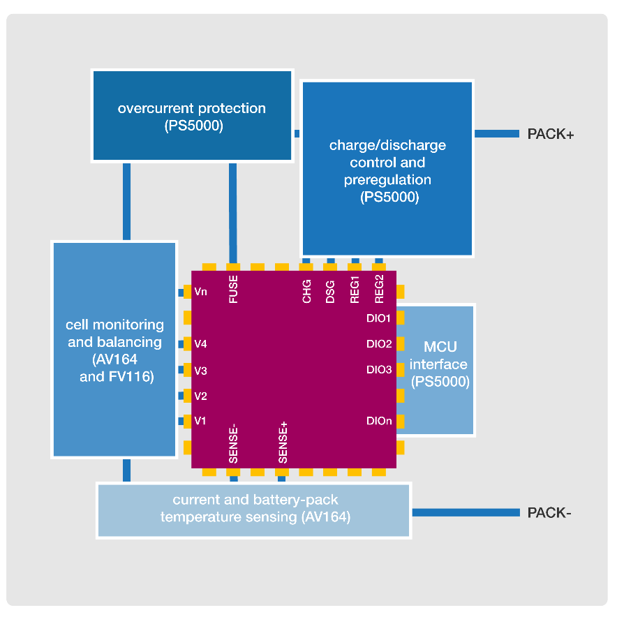
Figure 1. The various BMS functional blocks can be tested using the instruments listed in the parentheses.

BMS IC test requirements

The BMS ICs, in turn, require extensive testing to ensure they can accurately monitor the battery’s state of health. The required tests are becoming increasingly stringent as single BMS ICs handle more and more cells. Typical applications today involve up to 18 cells, but 20- to 24-cell stacks are becoming increasingly common. In addition, 28-cell stacks are starting to appear, with 32-cell stacks on the near horizon. Effective test requires instruments that can force and measure voltages of up to 150 V with accuracies of less than 100 µV on each cell-monitoring input.

Specific test functions include cell emulation, which can test the BMS IC without using real batteries. Cell emulation requires forcing a stable input voltage per simulated cell, and the instrument must establish voltage conditions dependent on the state of charge of the simulated cell. Cell-monitoring capability requires tests of the BMS IC’s analog-to-digital converters (ADCs) as well as ADC trimming. The tests must ensure that the BMS can accurately monitor current as well as read battery-pack temperature sensors. Finally, the tester must test a BMS IC’s cell-balancing capability by performing RDS-ON measurements at high common-mode voltages.

Test configuration variants

For cell emulation, a tester can employ one of several cell-simulation variants, each with cost and performance tradeoffs. The resistor ladder variant (Figure 2a) offers stable voltages and low noise and is inexpensive. However, it is subject to leakage currents that must be calibrated out, and the resistor values change as the resistors heat up. In addition, this variant will exhibit accuracy issues if the ADCs pull significant currents and the variant consumes considerable load-board space.

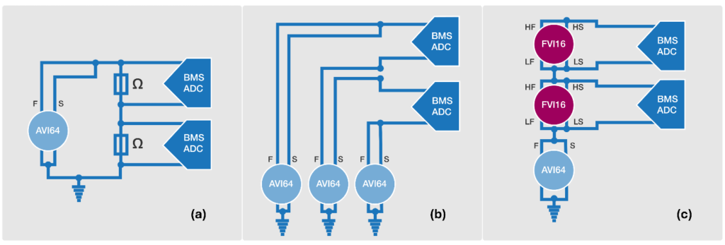
Figure 2. Resistor ladder (a), single-ended (b), and floating (c) variants can provide BMS cell simulation.

The single-ended variant (Figure 2b) simplifies load-board design, and some single-ended instruments can support differential voltage measurements. However, instrument accuracy can degrade at higher voltage levels, and compared to the resistor-ladder variant, the single-ended approach is resource-intensive. Finally, the floating variant (Figure 2c) employs a ground-based source as a pedestal on which floating instruments sit, allowing the floating instruments to operate at a lower range with greater accuracy. This variant provides stable and precise voltage at every channel and minimizes temperature sensitivity. However, it is also resource-intensive, so efficient multiplexing is required to keep the cost of test down. The V93000 supports all three variants, including hybrid solutions, to meet the individual requirements of the DUT and to best match available system configurations. 

BMS accuracy 

BMS accuracy is a key consideration that has implications for test. For safety, cells are ideally cycled between 90% charge and 10% discharge levels. To maximize battery lifetimes, respective values of 80% and 20% are often used. For typical lithium-ion chemistries, the change in voltage (ΔV) from 90% to 10% capacity can be approximately 500 mV, while ΔV from 80 to 20% is only about 100 mV. If BMS accuracy is within 5% (about 5 mV) for the 80%/20% characteristic, the usable cell capacity would be limited to 75%/25%.

To recover usable device capacity, a BMS would achieve a 1-mV device accuracy specification, and under the 10:1 rule, the ATE required to test it would need 100-µV accuracy. Floating instruments offer significant advantages in conducting tests with 100-µV accuracies compared with ground-based instruments, which do not offer sufficient resolution at high voltage levels.

Instruments for BMS IC test

Advantest offers several instruments for its V93000 automated test equipment (ATE) platform to facilitate the test of BMS ICs, including the Pin Scale 5000 digital card, the AVI64 analog and power card, and the FVI16 floating voltage/current (VI) source. In Figure 1, each instrument is listed in blue in the functional blocks that it can test.

The PS5000 can handle BMS IC digital test. It supports communications link and scan testing at speeds of up to 5Gb/s with 256 channels per card and a deep vector memory. Featuring a per-pin parametric measurement unit (PMU), the protocol-based board supports SPI, JTAG, I2C, and other digital I/O interfaces to test a BMS IC’s communication with a host microcontroller unit (MCU). In addition to testing a BMS IC’s digital I/O signals, the PS5000 can also test a BMS IC’s charge and discharge control signals and exercise the overvoltage protection.

The 64-channel AVI64 module employs Advantest’s universal analog pin architecture to extend the V93000 platform’s capabilities to include the testing of power and analog signals. The AVI64 includes per-pin arbitrary waveform generators (AWGs) and digitizers, per-pin high-voltage time measurement units (TMU), and per-pin high-voltage digital I/O. Furthermore, the AVI64 offers floating high-current and differential-voltage measurements as well as an integrated analog switch matrix and the ability to precisely measure voltage and current parameters simultaneously at every pin. It finds use in BMS IC cell monitoring and balancing test and can be used in all three variants shown in Figure 2. In addition, it finds use in BMS IC current and temperature sensing test.

Finally, each channel of the FVI16 floating-power VI source for testing BMS ICs can supply 250 W of high-pulse power and up to 40 W of DC to test the latest generation devices while conducting stable and repeatable measurements. The FVI16 features a digital feedback loop design, which provides improved source and measurement accuracy compared to systems that operate with traditional analog feedback. Sixteen channels with four-quadrant operation allow for efficient parallel testing. For high-voltage BMS testing, cell stack voltages of up to 200V can be achieved, which meets the requirements of today’s and foreseeable future BMS devices. Like the AVI64, the FVI16 finds use in cell monitoring and balancing test, and as shown in Figure 2c, it can work with the AVI64 in the floating cell-simulation variant.

Future BMS innovations

BMS technology is evolving to provide ever higher levels of performance and efficiency. One emerging innovation is the wireless BMS (wBMS), which promises to eliminate about 3 kg of wiring-harness weight of the total 35 to 90 kg of wiring harness weight in a typical EV (Figure 3). Wiring harnesses not only add weight, but they also add cost and complexity and take up valuable space, and harnesses and connectors are common failure points that can compromise reliability and safety.

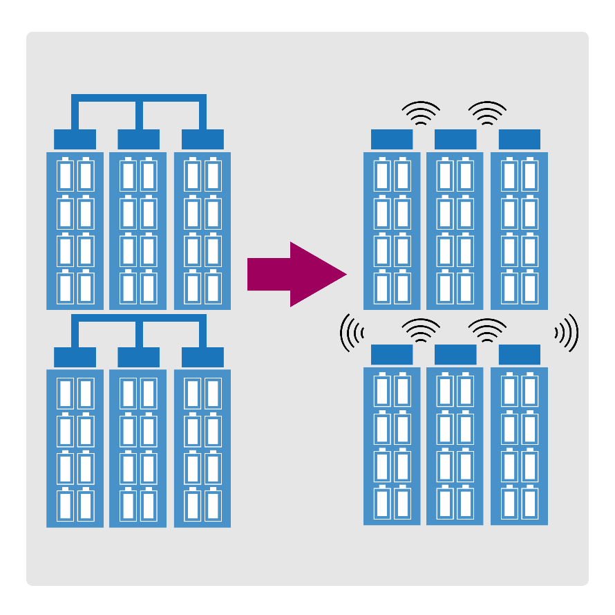
Figure 3. The wired BMS (left) faces competition from the wBMS (right), which saves space and weight and removes potential points of failure.

Compared with a wired BMS, a wBMS is estimated to save 90% of wiring weight and 15% of total battery-pack volume. Major vendors are already offering wBMS implementations. The V93000 platform has a long history of success in performing wireless test and is fully suited to performing both the RF and power/analog tests required for a wBMS IC.

Another emerging BMS innovation is electrochemical impedance spectroscopy (EIS), which improves on simple voltage and temperature measurements to determine the state of health, state of charge, remaining range, and other battery parameters. EIS involves applying a small AC voltage from less than 1 Hz to about 10 kHz across the battery and measuring the resulting AC current response to derive the frequency-dependent battery impedance. The impedance, in turn, indicates a battery’s internal processes, including ion mobility, charge transfer, and diffusion. EIS devices already on the market include a low bandwidth loop (less than 200 Hz), a high bandwidth loop, a precision analog/digital converter (ADC), and a programmable switch matrix, all of which can be readily tested using the V93000 ATE system.

Conclusion

The market for BMS ICs, which enable battery charging and protection, cell balancing, and state-of-charge estimation, is rapidly expanding, driven by electric vehicles and mobile tools. Scalable and flexible ATE is keeping pace with BMS advances, with instruments available for addressing higher voltages and finer accuracies, and it is well prepared to address the RF test challenges as wBMS technology advances. While this article focused on EV BMS applications, BMS technology has an equally important role to play in applications ranging from portable electronics to power tools. Advantest’s platform is suited for today’s and tomorrow’s testing requirements for all BMS devices, including those with RF capabilities.

Read More