Pages Menu
Categories Menu

Posted in Upcoming Events

First-Ever Virtual VOICE 2021 Developer Conference Receives Record-High Global Attendance

After being cancelled in 2020 due to the COVID-19 pandemic, Advantest held its 15th annual VOICE 2021 Developer Conference as an all-virtual event on June 21-23. The 3-day event attracted a record-setting 320 international attendees, with over half representing Advantest customers and partners. The 2021 conference drew participants from 53 unique companies hailing from 11 countries, including 20 new companies that had not previously experienced Advantest’s Developer Conference.

Yoshiaki Yoshida, CEO of Advantest Corporation, and Doug Lefever, CEO of Advantest America Inc., kicked off the conference by welcoming event attendees. This year, the Virtual VOICE program included 68 technical presentations from 21 companies covering eight topical tracks, and 22 technology kiosks highlighting Advantest’s latest test innovations.  The event incorporated 32 live sessions, giving speakers and attendees the opportunity to interact and exchange valuable information on best practices, test challenges, applications and solutions.

Additionally, Virtual VOICE featured a 13-company strong Partners’ Expo headlined by Alliance ATE and ISE Labs, two dynamic keynote speakers, and a featured industry talk on the semiconductor market by G. Dan Hutcheson of VLSIresearch Inc. VOICE concluded with an award ceremony and custom music video performance by classically trained violinist Gabi S. Holzwarth. 

Best Papers and Best Kiosk Award

Through an online poll, attendees voted to select the top two technical presentations and the best technology kiosk. 

Best Paper Award: 

  • “HSIO Loopback: The Challenges and Obstacles of Testing 112 Gbps” / Dave Armstrong – Advantest, Don Thompson – R&D Altanova
  • “Automotive Keyless Entry System-on-Chip Test Methodologies and Techniques” / Jonvyn Wongso, Krishna Vangapalli, and Daniel Marstein – Microchip Technology, Philip Brock and Louis Benton – Advantest 

Best Kiosk Award:

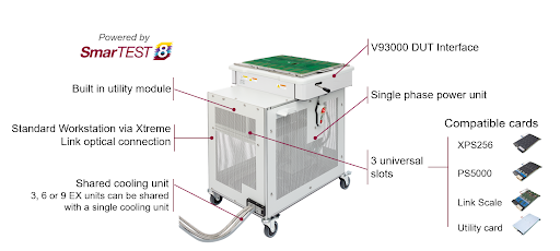
  • “EXA Scale Infrastructure and Utility Card” / Helmut Schmid and David Butkiewicus – Advantest

Visionary Award:

  • Derek Lee – NVIDIA 

The annual VOICE Developer Conference is made possible by the extensive organizational work of a Steering Committee, comprised of volunteer representatives from Advantest and its worldwide customer base and the support of event partners and sponsors

Check out the Virtual VOICE event highlights video here on LinkedIn.

We look forward to hosting VOICE 2022 as an in-person event in Scottsdale, AZ, USA on May 17-18, 2022. Watch the VOICE website for more details: https://voice.advantest.com/

Read More

Posted in Featured

Advantest’s Hadatomo™ Z Photoacoustic Microscope Wins Laser Industry Encouragement Award

Advantest’s Hadatomo™ Z photoacoustic microscope received a Laser Industry Encouragement Award at the 13th Industry Awards sponsored by the Laser Society of Japan.

The Laser Society of Japan Industry Awards recognize “excellent achievements contributing to the development of the domestic laser-related industry in the practical application, and the dissemination of laser-related products and technologies,” according to the Society. Among several award categories, Encouragement Awards are given to products with notable potential for future market development.

Advantest’s Hadatomo™ Z simultaneously images the oxygen saturation of blood vessels with dual-wavelength photoacoustic technology, and dermal structure including skin texture, pores, and sebaceous glands with ultrasound. Accurately imaging vascular mechanisms up to a depth of 3 mm in the dermis makes it possible to observe vasodilation and blood circulation stimulation in near-real time. An optional dual-wavelength laser that can distinguish between melanin and blood vessels is also available. Currently, the product’s main applications are cosmetology and dermatological research, but its selection for the Encouragement Award underlines its future potential as a medical device. At the present time, the product is a scientific instrument, not an approved medical device.

This award reinforces Advantest’s commitment to developing the company’s photoacoustic technology further, so that the Hadatomo™ Z can contribute to the treatment and prevention of skin diseases.

The 13th Industry Awards of The Laser Society of Japan for fiscal year 2021

https://www.lsj.or.jp/en/the-13th-industry-award-on-the-laser-society-of-japan-in-fy-2021/


Read More

Posted in Featured Products

New TAS74000TS Measurement Solution Enables Materials Characterization for Beyond 5G

Advantest introduced a high frequency resolution option for its TAS7400TS terahertz optical sampling analysis system. It features excellent cost performance and ease of operation, and a new option that provides a groundbreaking measurement method for high-frequency characteristic evaluation of radio wave absorbers and base materials, which are indispensable for Beyond 5G / 6G next-generation communications technology and for the millimeter-wave radar technology used in ADAS (advanced driver assistance systems). 

Vector network analyzers (VNAs) have been widely used to evaluate the transmission characteristics (transmittance, reflectance) and complex permittivity of various materials in the millimeter-wave and high-frequency regions. But in recent years, it has become important to evaluate these characteristics over wider bandwidths, raising issues with VNAs on account of the time and effort required to set and calibrate each frequency band.

Advantest’s terahertz optical sampling system addresses these issues by enabling batch measurement over a wide band, utilizing pulsed electromagnetic waves. Measurements are now possible with a compact optical sampling system (measurement environment), saving on cost and space. It is also possible to analyze surface frequency characteristics with the mapping measurement option. Furthermore, the frequency resolution and scan speed of the new option are 5x that of the previous product, making this an optimal solution for evaluating the high frequency characteristics of new materials.

The solution will be exhibited at JASIS, from November 8th to 10th, and at MWE 2021, from November 24th to 26th.

Read More

Posted in Top Stories

Automotive Keyless Entry SoC Test Methodologies and Techniques

By Philip Brock, Applications Engineer & Consulting Manager, Louis Benton, Jr., Applications Engineer & Consulting Director, Advantest, and Jonvyn Wongso, Technical Staff Test Engineer, Microchip

Note: This article excerpts content from the Virtual VOICE 2021 Best Paper, voted on by conference attendees. Jonvyn Wongso, Daniel Marstein & Krishna Vangapalli from Microchip Technology co-authored the original paper, and their research and development efforts were invaluable to this project.

Passive Entry Passive Start (PEPS) technology has become standard in the automotive market for keyless operation. A secure wireless communication system, PEPS enables to lock and unlock the vehicle, start and stop the vehicle without physically using the key. Electronic functionality embedded in the key fob to interact with the vehicle (see Figure 1) includes passive start and stop, passive lock, remote keyless entry, immobilizer, key fob wake-up, and key fob localization. These functionalities are controlled by the primary modules embedded within the fob itself. The immobilizer provides access to start the vehicle when the key fob’s battery level is low by placing the fob at the start button and pressing it.

Figure 1: This diagram illustrates how components within the key fob correspond to functionality in the car itself.

The PEPS-to-vehicle ecosystem requires several key modules to function that includes a low-frequency (LF) transmitter, an immobilizer, a Radio Frequency (RF) transmitter (key fob) and transceiver (vehicle side), as well as a microcontroller (MCU). Each module in the key fob poses specific testing challenges and restrictions, necessitating a test plan and flow optimized for the testing of the key fob’s circuit, as shown in Figure 2. 

Figure 2: The key fob architecture depicts the main components within the key fob and a representation of how each component is tested on the Advantest V93000 test system.

The coverage percentages at the upper right in Figure 2 represent the overall test flow’s test time. Approximately two-thirds of the test coverage is dedicated to the LF structure (analog) and the MCU (digital), with another 19 percent focused on power management and parametric tests. The remaining 6 percent of the test coverage involves testing of the RF module with transmission functionality at sub 1 GHz band with no RF reception capability.

The combination of test requirements to accommodate all the different technologies housed within the PEPS key fob makes it an ideal device for demonstrating the versatility of the Advantest V93000 SoC test platform, including the AVI64 and PS1600 pin cards. A test solution is designed with comprehensive methodologies to test every module in the key fob. The balance of this article summarizes the key aspects of the test approach.

PEPS test methodology elements

Digital

Digital testing utilizes two standard methods to communicate to the IC:

  • Serial programming interface (SPI) – Standard communication protocol is used to test all non-MCU (non-digital) structures via direct access to the RAM. However, due to the slow communication speed compared to HVSP protocol, the programming time to the EEPROM is approximately 10ms per byte.
  • High-voltage serial programming (HVSP) – Used for FLASH and MCU core test with fast access to the EEPROM, this proprietary protocol is much faster than SPI, with a FLASH and EEPROM programming time of 3 to 4ms per page (each page is 16 bytes long).

One key digital test that has to be performed is to measure the time to program a page to the FLASH (16 bytes). The page program completion time varies between devices. The typical test method to measure and detect the end of the programming time is by implementing a match loop counter opcode in the pattern vector as the device asserts a state of a pin to high when the programming event has completed. However, the implementation of this method prohibits the use of the PS1600’s Time Measurement Unit (TMU) function on the same channel pin in parallel to measure the page program time accurately.

The test methodology developed involved the use of the Rapid Development Interface (RDI) API, a code structure that wraps Advantest’s standard application programming interfaces (APIs). The API is based on object-oriented programming that encapsulates firmware commands, enabling seamless execution of multiple commands. This creates a competitive advantage by dramatically streamlining the software development, and with the V93000’s multiport capability, it enables higher timing resolution that can be achieved on a specific pin or pin group. The use of the comparator functionality allows to strobe for a level change in the signal for a fixed amount of time.

Power Management

The Brownout detection circuit in the PEPS is a challenge to test to achieve optimized test time. In a typical test method, a voltage sweep is conducted from high to low to detect the brownout state threshold, followed by a voltage sweep from low to high to search for the recovery threshold level. An experiment was conducted with the implementation of four different test methodologies to determine the most optimized method to test the Brownout Detection circuit, summarized in Figure 3. In summary, the implementation of the Per Pin Parametric Measurement Unit (PPMU) as the Arbitrary Waveform Generator (AWG) yielded the fastest test time with minimal test instrument latency dependencies.

Figure 3: Investigation of four different brownout detection methodologies – PPMU as AWG methodology consumes a fraction of the test time in comparison with the other three options

Low Frequency Test

The Receiver Signal Strength Indicator (RSSI) circuit in the key fob indicates the proximity and location of the key fob with respect to the vehicle. The 3D LF pins are transponders with signal transmission and detection  at a frequency of 125 kHz with detection amplitude levels as low as 1.0 mV peak differential. The LF test requires a complex on-board circuitry in order to source AWG amplitude levels from 1 mV up to 8 V peak. Due to the real estate demand from the load board to implement these circuits with amplitude ranges, the extra-large size load board is used, extending out on both sides of the tester’s field. The RSSI value may only be read out after the completion of conversion of the LF signal level from a specific register in the device. In addition, there is a register that may be continuously read to check for status of the RSSI conversion.

Therefore, the proper test methodology for this test is to implement the Condition Go-No-Go (COGO) API from RDI to continuously check for the status of the conversion. This method corresponds to the device’s application. However, due to the inherent long latency to judge each event using COGO (described in Figure 3), a one-time fixed time delay was implemented prior to the readout of the RSSI conversion.

The other primary LF test involved the transponder, which is used for the immobilizer. The key fob that is placed at the start button of the vehicle will be energized by the vehicle’s coil that is located around the start button to enable communication between the key fob and the vehicle. This test requires both the AWG and Digitizer (DGT) instruments to source and capture the modulated waveform on the LF pins.

The communication between the key fob and the vehicle compromises of three stages as shown in Figure 4 – startup (energizes key fob), write mode (vehicle transmit authenticated message to key fob) and read mode (key fob responses with another authenticated message). The post processing of both the sourced and received waveform uses custom Digital Signal Processing (DSP) functions along with built-in V93000’s DSP APIs. 

Figure 4: Transponder communication between key fob and vehicle on LF pins on key fob.

RF Test

The Amplitude Shift Keying (ASK) modulation is used to transmit RF authenticated signal from the key fob to the vehicle. It is critical to test the duty cycle of the modulated signal that has a period of 12.5 us, toggled by an external pin when set in test mode. The device itself operates at a 2 us period. Therefore, multiport has to be implemented for the sequencer to drive two groups of ports at different periods. This test methodology also includes RF site interlacing technique, taking advantage of the V93000’s eight-site parallel test capability with 2 RF FE24 cards. Figure 5 illustrates the test criteria and methodology employed. Post-processing involves the capture of complex waveform, conversion of the waveform to rms in order to create the burst envelopes, performing moving average to filter out noise and searching for all falling and rising edges to calculate the duty cycle. 

Figure 5: The transmit ASK duty cycle test methodology is summarized here.

Software/hardware techniques

The LF testing requires sharing of the AWG and Digitizer instruments (MCE 4 source and 4 measure units) across 8 sites, thus increasing test time and reduces multisite efficiency. The implementation of SEMI_PARALLEL block in the test method enables execution of a single test cycle, hence maximizing multisite efficiency. Sequencers connected to AWG and DGT are placed in the SEMI_PARALLEL block as shown in Figure 6. Method 1 is the most common implementation. However, the setup pattern will be executed more than once on the same site. In contrary, method 2 is the least efficient but may be an option if the setup pattern may only be executed once to each site to avoid change of the state of the device.     

Figure 6: Shown here are the two most common SEMI_PARALLEL block test flow methods for shared resources.

Another test method technique implemented as part of the test solution includes the use of both RDI and MAPI APIs to resolve per site device failure on a specific mode or event as shown in Figure 8. RDI is used for the initial generation and execution of the pattern. MAPI APIs are subsequently used to re-execute the RDI generated pattern to specific failed sites. This method allows the recovery of the device(s) within the test method to save test time and not applying stimulus and retesting already passed sites.

Figure 7: The combination of RDI and MAPI usage enables device per site failures to be resolved.

On the hardware side, the use of relay driver circuit (SN74LS04DR followed by MDC3105LT1G) enables the drive of eight relays simultaneously such as G3VM-41QR10TR05 only by using a single utility pin. This technique enables the implementation of many circuit paths on the load board but omits the need of a PMUX card in the tester. Subsequently, the test load board design requires calibration of every signal path and circuit for each test site. There is an on-board EEPROM that stores the calibration offset and losses. Due to the limitation of memory space in the EEPROM, every calibration value is compressed using IEEE754 floating point standard. Depending on the accuracy requirement, this method enables greater than 50-percent compression rating of a decimal value. 

In summary, there are many challenges in both hardware and software development to create a test solution for optimized test time and efficiency, as summarized in Figure 8.

Figure 8: Summary and challenges of PEPS key fob test solution.

Since this device is targeted for automotive application, it has to be tested at cold, room and hot temperature ranges. Temperature variations affects the performance of the circuitry on the load board and has to be calibrated for each temperature range. The MCU core has to be tested at multiple different voltage level that requires synchronization of the pattern sequencer for each level change. In addition, testing the LF circuit requires extensive changes in the AWG’s amplitude level that requires additional setup and execution time that may increase test time and lower efficiency.

Read More

Posted in Top Stories

HSIO Loopback Turns Challenges into Opportunities for Test at 112 Gbps

By Dave Armstrong, Principal Test Strategist, Advantest, and Don Thompson, Senior Director of Engineering, R&D Altanova

For both PCIe and Ethernet (IEEE 802.3) signals are getting mighty small. With PCIe 5 reaching 32 Gbps (NRZ at 32 GBaud) and 802.3 reaching 112 Gbps (PAM4 at 56 GBaud), typical eye-mask limits are shrinking. Consequently, test requirements for high-speed I/O (HSIO) test are becoming daunting.

HSIO test involves measurement of Tx eye height and width, confirmation that a receiver can detect a low-level signal, and confirmation that continuous time linear equalization (CTLE) is effectively compensating for insertion loss. In addition, the test must verify bit error rate and confirm that a receiver can receive an off-frequency or out-of-phase signal. Yet another requirement is DC access for continuity and scan test.

Traditionally, HSIO loopback has been the preferred approach to HSIO test, with a simple wire or capacitor connecting a DUT’s Tx to Rx inputs. Loopback itself comes in various forms. The simplest form is internal loopback in which the device talks to itself and never exercises the transceiver circuitry; it can test internal logic only.

Another method is AC-coupled external loopback which does exercise the I/O circuitry, but like internal loopback, it does not perform Tx/Rx eye tests, and it does not test pre-emphasis and equalization. AC-coupled loopback is easy to lay out on a DUT board, but the signal level the Rx receives is too low loss / too hot, making the test too easy. Similarly, when connecting channel pairs for loopback tests, the Tx/Rx pairs share the same PLL/DLL, again making the test too easy. 

There are some workarounds that can be used on an AC-coupled external loopback. Long circuit-board trace lengths could help make AC-coupled test more realistic, while connecting the Tx of one signal pair bank to the Rx of another would mitigate the problems of a shared PLL/DLL. And the addition of bias tees loopback circuits would support DC and continuity (Figure 1).

Figure 1. AC-coupled external loopback test with bias tees for DC test.

However, these loopback tests do not provide sufficient visibility into the DUT that would aid in diagnosis, making them ineffective, particularly at speeds as high as 112 Gbps.

With the addition of some high-performance MultiLane instruments, one can improve on the simple loopback tests significantly. The Advantest V93000 platform supports two very different approaches for HSIO test: 16-Gbps test with the Advantest’s Pin Scale Serial Link (PSSL) card or 112-Gbps test with the MultiLane test-head resident instrumentation. 

The MultiLane approach supports a 112-Gbps PAM4 bit-error-rate tester (BERT). Based on a benchtop BERT, the AT4039E is configured as an eight-lane cassette that fits under a V93000’s DUT board, keeping signal paths short. In a similar fashion, the AT4025-50, which is the heart of the approach suggested in this paper, is a 50-GHz digital sampling oscilloscope (DSO), configured with eight channels per cassette, with 32 channels maximum per system. This complements the BERT and also fits underneath the V93000’s DUT board. The different types of instrumentation have their own advantages and disadvantages, each leaving some gaps in measurement coverage (Table 1).

Table 1. Instrument-based test capabilities for NRZ and PAM4 signaling.

A combination of instruments and a technique we call “BIST plus scope-sampled loopback” can fill the gaps while keeping instrumentation costs low and test times short. BIST plus scope-sampled loopback adds a splitter that provides a signal path to the DSO (Figure 2). 

In contrast to the PSSL or a BERT where test patterns originate and are received, the scope-sampled loopback technique makes use of the DUT’s BIST circuitry to generate a pseudo-random bit stream. The DSO can monitor this data stream while it is looped back to the DUT receiver in order to provide a comprehensive report on device performance during this real-world usage. Not only does this provide the user with valuable parametric data on the SerDes performance, it allows one to clearly differentiate between Tx and Rx problems. This approach also provides 6 dB of attenuation, more closely mimicking actual operation than does the standard AC-coupled loopback test, thereby overcoming the drawback of a test being too easy. Adding a programmable attenuator can provide an even more thorough test.

Figure 2. AC-coupled loopback test with a splitter providing access to a digital sampling oscilloscope.

The sampled-loopback technique does require some DUT-board real estate. One example of an AC-coupled loopback circuit with a splitter paired with an attenuator requires about 234 mm2 vs. 48 mm2 for an AC-coupled implementation with bias tees. The valuable data a DSO can capture using the technique can justify the additional DUT-board real-estate cost.

Sampled loopback also poses DUT-board layout challenges regarding trace losses and via impedances at 112-Gbps frequencies.  Tester signals connect on the bottom of the DUT board and make their way to a socket on the top.  This requires multiple vias and several inches of matched PCB traces to ensure that each lane sees the exact same interconnect length and attenuation (Figure 3).

Figure 3. DUT board showing insertion loss and impedance discontinuities.

The margin of error is small, requiring high-speed dielectrics (lossy dielectrics are sometimes used to stress the link) with trace widths typically between five and seven mils and prioritizing loopback circuit placement to keep trace lengths kept short. 

DUT boards are typically between 0.200 in. and 0.300 in., which pose signal-integrity challenges for vias.  Tuned-impedance vias are required to reduce insertion loss and must be a key focus for successful DUT-board designs at 112 Gbps. Finally, socket performance is also critical, and the socket cannot be an afterthought.

High-speed design requirements mandate effective SI simulation and optimization with all circuits modeled and included in the simulation well before the design is completed. 

Once fabricated, careful VNA measurements should be performed to confirm that design goals were met. Fortunately, a tightly integrated design-to-fab process can meet the requirements of DUT-board layout to support the BIST plus sampled loopback technique. High-frequency design validation closes the control loop on the design-to-fab process, providing proof of simulation accuracy, proof of board fabrication execution, and proof of final board performance. 

Initially, adding sampled loopback on all lanes supports the use of many DSO channels during characterization to speed data gathering. In production, you can make use of the characterization data to determine which lanes should continue to be monitored. Ultimately, for a mature product, the hope is that the DSO is no longer needed to monitor any channels.

Sampled loopback offers several advantages. For example, production software can support sampled loopback with the addition of scope code to check the DUT output.  In addition, the scope serves as a calibrated observer, a function not available with a device communicating with itself in a standard loopback test. PLL/DLL/VCO issues are some of the most common issues with SerDes interfaces and are best detected with the scope approach.  Finally, scope measurements are much faster than BERT measurements. 

Table 2 shows the scope sampled loopback technique closes the gaps in Table 1.

Table 2. Test and measurement gaps closed through the use of the BIST plus scope-sampled loopback technique.

Conclusion

In summary, early data and experience suggest that simple internal loopback, which tests only the ability of a part to talk to itself, is inadequate for testing many high speeds ICs. The addition of a calibrated external instrument such as the MultiLane DSO via sampled loopback provides the ability to identify problems that would otherwise be missed at 112 Gbps. 

Advantest can apply its years of experience in high-speed digital test to help you implement a BIST plus sampled-loopback strategy, and R&D Altanova can assist with the design of the very complex DUT boards supporting 112-Gbps data rates for the V93000 tester.

Reference

This article is based on the award-winning VOICE 2021 presentation “HSIO Loopback—The Challenges and Obstacles of Testing at 112 Gbps,” by Dave Armstrong, Advantest, and Don Thompson, R&D Altanova. 

Read More