Pages Menu
Categories Menu

Posted in Upcoming Events

Advantest’s 2022 VOICE Developer Conference Concludes with Record Attendance

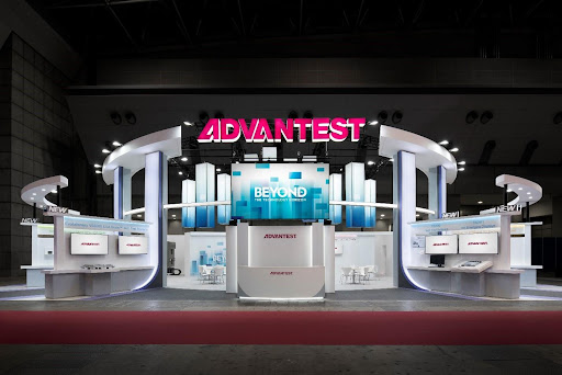
Advantest held its VOICE 2022 Developer Conference on May 17-18 in Scottsdale, Arizona, achieving maximum attendance and sponsorship capacity. Over 300 people attended the event, the majority of whom were Advantest customers and partners. The 2022 conference represented over 60 companies and included presentations of more than 60 technical papers over two days.

VOICE 2022 received 119 abstract submissions from 31 companies across 13 countries. A total of 66 papers were accepted for presentation during the technical breakout sessions, half of which were written or co-authored by customers.

In addition to the technical sessions, VOICE featured a Partners’ Expo, three highly rated keynote speakers, and a first-time “fireside chat” conducted between G. Dan Hutcheson, vice chair of TechInsights, and Manish Bhatia, executive vice president of Global Operations at Micron.

Through the VOICE mobile app, attendees voted to select the best technical presentations and best technology kiosk.  A Visionary Award was also named for ongoing, sustained support of VOICE by a customer.

Best Paper

  • “New ATE Testing Techniques Using PCI-Express with Link Scale-PCIe to Solve Scan, Structural, Protocol and Third-Party Integration Challenges” / Brendan Tully—Amazon, Mike Kozma—Advantest 
  • “Migrating the Test of Medium Power Mainstream SOC Devices Using UHC4T/DPS128 to a Single XPS256 DPS Solution” / Stefan Walther and Linda Hänel—Advantest 

Best Kiosk Award

  • “ACS Edge 2.0” / Sonny Banwari and team—Advantest 

Visionary Award

  • Gabriel Tellechea—AMD 

VOICE is made possible by the organizational work of a Steering Committee, made up of volunteer representatives from Advantest and its customers, and the support of event sponsors, which featured 22 companies, including two new participants this year.

We look forward to hosting VOICE 2023 on May 9-10 in Santa Clara, California. Keep an eye on the VOICE website for more details: https://voice.advantest.com/

Read More

Posted in Featured Products

Advantest Introduces Industry’s First Flexible DUT Interface 

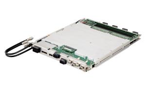
Advantest launched its DUT Scale Duo interface for the V93000 EXA Scale SoC test systems, enabling the industry’s highest level of parallelism for testing advanced semiconductors. With this revolutionary interface, the usable space on DUT boards and probe cards is increased by 50 percent or more while wafer probe and final-test setups can accommodate component heights that are more than three times taller.

Advantest offers the industry’s first DUT interface with the capability to adapt either to the existing standard DUT board or probe card size or to switch to the new, significantly larger size. Using a unique sliding mechanism, users can effortlessly switch back and forth between both formats to adapt to specific application requirements.

Along with the new interface, a new super-stiff extended bridge achieves superior deflection performance in direct-probing setups. The unit’s universal design gives it the versatility to support a wide range of applications including digital and RF device testing. With its sophisticated sensing capabilities, the extended bridge delivers the industry’s best planarity and high manufacturing yield, ensuring highly accurate positioning and verification of probe card clamping.

“Our new DUT Scale Duo enables the next stepping in parallelism while embodying Advantest’s continuing emphasis on system compatibility by allowing users to utilize their existing DUT boards and probe cards with a new interface,” said Advantest’s General Manager and EVP, Jürgen Serrer. “In addition to protecting customers’ investments, our approach to delivering the most efficient test solutions also offers flexibility and simplifies fleet management on the test floor.”

Read More

Posted in Featured Products

Advantest Enables PCIe Gen 5 NVMe & CXL Device Testing on Proven MPT3000 SSD Test Systems

Advantest announced that its MPT3000 solid-state drive (SSD) test systems are the industry’s first with the ability to test PCI Express fifth-generation (PCIe Gen 5) devices, including those utilizing the new Compute Express Link (CXL) interconnect standard. To help drive product introduction, qualification, and volume production demands associated with PCIe Gen 5 NVMe & CXL devices, several leading memory device makers have purchased multiple MPT3000 products, including MPT3000ES engineering systems, MPT3000HVM high-volume manufacturing testers and device interface boards.

PCIe Gen 5 enables high-speed data transmission—essential for data centers, artificial intelligence (AI), and 5G applications. CXL is an open industry standard memory interconnect that builds on the physical and electrical interfaces of PCI Gen 5 to provide high-performance connections across memory types. 

Advantest designed its flexible MPT3000 systems to meet testing needs for enterprise and client SSDs, helping shorten customers’ time-to-market. In addition to CXL test, key MPT3000 capabilities include testing up to 32 Gbps, increased sideband and high-speed support, and improved temperature management for high-wattage drives.

“We are committed to driving memory and storage test innovation by developing the first systems and boards that will enable testing for both PCIe Gen 5 CXL and NVMe SSDs,” said Indira Joshi, vice president, SSD Test Division, Advantest America. “By expanding our proven MPT3000 system’s capabilities to address PCIe Gen 5 CXL, we are well positioned also to expand our relationships with important customers in the memory market.”

Read More

Posted in Q&A

CREA Brings Power Semiconductor Know-how to Advantest 

By GO SEMI & Beyond staff

In June 2022, Advantest announced its acquisition of Italian ATE company CREA. As leading developer and provider of equipment for testing power semiconductors, CREA brings vital capabilities to Advantest’s portfolio of test solutions. To delve further into the acquisition and how it will benefit Advantest’s customers, we talked with Fabio Marino, director of Advantest’s Power, Analog and Controller Business.

Q: What prompted Advantest to pursue adding power semiconductor test to its capabilities?

A. When considering any strategic action, we are guided by our Grand Design, which defines the commitments and strategies needed to further our goal of enabling leading-edge technologies by adding customer value throughout the semiconductor value chain. This goes hand in hand with looking at relevant market and technology advancements.

Until recently, the high-voltage power device market was a niche, low-volume market. However, fast-growing adoption of electric vehicles (EVs) is driving heightened demand for discrete components. Demand for power semiconductors is growing significantly in response to the need to utilize power more efficiently for EV applications – we expect the market for these devices to grow by 10x over the next eight years. As a result, we realized we would need to pursue this market by bringing power semiconductor test into our portfolio.

Q. Why was CREA selected for acquisition?

A. While there are several suppliers of power semiconductor testers, we determined that CREA was the best fit for Advantest because of several factors, including its:

  • Superior technology platform, which covers both static and dynamic power test, proven over 30 years;
  • Expertise in compound semiconductors, including silicon carbide (SiC) and gallium nitride (GaN);
  • Strong installed base, with more than 200 testers installed at semiconductor makers worldwide; and
  • Synergistic business approach, viewing customers as partners, with the goal of full solutions and support for customers’ testing needs.

Q. How is CREA being integrated into Advantest?

A. CREA will remain headquartered in Italy as a wholly owned subsidiary of Advantest Europe, within our ATE Business Group. CREA’s management team is continuing to run the subsidiary, with Advantest providing additional team support as needed.

Q. Can you talk about the company’s portfolio a bit? What makes it such a strong addition to Advantest’s offerings?

A. CREA’s proprietary technologies are key to its power device test capabilities. These include its PCI probe card interface, vital for known good die (KGD) and wafer test; LSI low stray inductance technology, essential to reduce parasite effects during test; and RTH remote test head, which works in conjunction with LSI to achieve high performance up to 1.5m away from the tester to enable handler and wafer prober use for mass production.

These products are integrated into CREA’s tester line, which comprises three product families:

  • The MT100 family, with a range of voltages and currents, which covers test requirements for static parameters from dies to complex configuration modules;
  • The MT200 family, which adds dynamic and combined parameter test to reach ranges up to 10 kV and 10 kA; and
  • The MT300 family, designed to satisfy the market’s most stringent requirements.

The CREA portfolio also includes turnkey solutions incorporating its fixture system, as well as manual and automated handlers.

Q. How do customers view the acquisition?

A. Customer reaction has been very positive. CREA has developed an excellent reputation over its 30 years of existence, and customers understand the strengths their test systems bring to Advantest and how they benefit in return. CREA will retain, to a large extent, the fast response time and flexibility it enjoyed as a standalone company, while, as a subsidiary of Advantest, its development team will have access to our broad corporate resources and collective knowledge base, which will benefit their ongoing technology advancement efforts. We’re excited by the opportunities the CREA acquisition provides for increasing customer value by enabling us to jointly develop new solutions to meet customers’ future demands.

In addition, by integrating CREA’s product lineups, development capabilities, customer base, and outstanding technical team into Advantest, we’ll be able to expand our solutions for power semiconductors. This will benefit both our company and our customers by allowing us to directly contribute to the broad goal of realizing a Net-Zero society. 

Q. What’s the bottom line for Advantest with this acquisition?

A. We intend to be a key player in the high-power market, and we believe that the technology CREA brings to the table will give us a competitive advantage, allowing us to have a significant market share. Moreover, CREA’s synergy with our established customer relations and global account setup will combine to help drive sales for these power semiconductor test products. 

Read More

Posted in Top Stories

A Customized Low-Cost Approach for S-Parameter Validation of ATE Test Fixtures

This article summarizes the content of a paper jointly developed and presented by Advantest and Infineon at TestConX 2022.

By Zhenhua Chen, Senior Application Engineer, Advantest Europe

Device under test (DUT) fixtures for ATE system pose several verification challenges. Users need to measure the DUT test fixture quickly and easily, while making sure the measurements mimic the ATE-to-test-fixture interface performance and determining how to handle DUT ball grid array (BGA)/socket measurement. These challenges are further highlighted by the unique issues faced individually by probing on the ATE side and on the DUT side of the test fixture.

Usually on the ATE side there are only two types of interconnect: coaxial connectors, which can be easily probed using the appropriate cable assembly; and spring pin vias, which are more complicated to probe. A spring pin cable assembly with a coaxial connector or a probe/adapter can be used. On the DUT side, the BGA ballout of the device (pitch/pin-out) presents the first challenge to probing at the socket. The second challenge is that including the socket in the measurement requires compressing the spring pins, elastomer, etc. in the socket. This can be achieved with a properly designed interposer.

The traditional approach to addressing these issues is to utilize a generic commercial probe station, with a pogo via adapter on the top side of the load board and BGA pad on the bottom side. These stations are very large and costly, and using them requires prior experience and expertise. On the other hand, to “MacGyver” a solution, the user would need to obtain an ATE test fixture mechanical interface and assemble it for manual use, then modify a standard spring pin ATE cable assembly by cutting off the unified pin connector and attaching individual coaxial SMA connectors. This so-called solution, while less cumbersome than a commercial probe station, is not practical for quick and easy implementation, as it is time- and labor-intensive and difficult to replicate.

Custom probing kit to the rescue

Advantest has developed a cost-effective solution to these challenges: our custom probing kit for V93000 DUT test fixtures that can be easily assembled and implemented as a desktop ATE test fixture. Figure 1a shows what the user receives in the kit, while Figure 1b shows additional parts needed and illustrates how the DUT board is positioned on the bracket. Figure 2 shows an example of a completed, installed assembly.

Figure 1. Advantest’s custom probing kit includes everything needed to build a cost-effective desktop V93000 ATE test fixture. [Board image courtesy of Infineon]

Figure 2. Advantest’s probing kit can be quickly and easily assembled and installed on the user’s desktop, as shown in this example, with cables that can connect to any instrument necessary. [Board image courtesy of Infineon]

Addressing the de-embedding challenge

The IEEE 370-2020 standard incorporates parameters for measuring DUT performance, recognizing the critical importance of the test fixture in this capacity. This includes de-embedding, which the standard defines as “the process of removing fixture effects from the measured S-parameters [scattering parameters].” ATE test fixture de-embedding is not trivial; the measurement reference location is critical for de-embedding to be successful. The de-embedding reference point needs to be a location with stable electromagnetic (EM) fields. The de-embedding software will always de-embed whatever data is provided, but this doesn’t automatically mean that the de-embedding is physically correct.

Several de-embedding technique options are available. For ATE PCB test fixtures, we suggest the 2X-Thru approach, which requires a de-embedding test structure and is supported by the 370-2020 IEEE standard. The 1X-Reflect approach requires a short or/and open, and is not supported by the 370-2020 IEEE standard. Figure 3 provides an example of successful de-embedding.

Figure 3. This de-embedding example utilized the 2X-Thru approach.

As Infineon product engineer Manfred Brueckl noted, “De-embedding ATE test fixtures is a challenge that has typically required cumbersome or costly solutions. With this probing kit, Advantest has created a much-needed way to address this challenge that is both space-saving and cost-effective.”

Conclusion

Measuring the ATE PCB test fixture is a critical step that can save the test engineer a great deal of time later during initial application turn-on. This is especially critical for applications where test fixture S-parameters are required for the de-embedding process. Different probing approaches are possible to address this challenge, but because of the specific mechanical design associated with an ATE platform, using a customized probing setup provides the best cost/capability trade-off. Advantest has developed this setup in a kit that is easily assembled and implemented to accommodate a user’s specific requirements.

References

Books

  • Jose Moreira and Hubert Werkmann, “Automated Testing of High-Speed Interfaces,” 2nd Edition, Artech House 2016.
  • Luc Martens, “High-Frequency Characterization of Electronic Packaging,” Kluwer Academic Publishers 1998.
  • Scott A. Wartenberg, “RF Measurements of Die and Packages,” Artech House 2002.

Papers on Socket Probing

  • Heidi Barnes et al., “Performance at the DUT: Techniques for Evaluating the Performance of an ATE System at the Device Under Test Socket,” DesignCon 2008
  • Heidi Barnes et al., “Advances in ATE Fixture Performance and Socket Characterization for Multi-Gigabit Applications,“ DesignCon 2012.
  • Jose Moreira, “Design of a High Bandwidth Interposer for Performance Evaluation of ATE Test Fixtures at the DUT Socket,” ATS 2012.

Papers on De-embedding

  • Jose Moreira et al.,“DUT ATE Test Fixture S-Parameters Estimation using 1x-Reflect Methodology,” BITS China 2017.
  • Heidi Barnes et al.,“Verifying the Accuracy of 2x-Thru De-Embedding for Unsymmetrical Test Fixtures,” EPEPS 2017.
  • Heidi Barnes et al., “S-Parameter Measurement and Fixture De-Embedding Variation Across Multiple Teams, Equipment and De-Embedding Tools,” DesignCon 2019.
  • Xiaoning Ye et al.,“Introduction to the IEEE P370 Standard and its Applications for High-Speed Interconnect Characterization,” DesignCon 2020.
Read More